In the high-stakes world of semiconductor manufacturing, where a single speck of dust can spell disaster for a multi-million dollar production line, the protection and transportation of silicon wafers is paramount. At the heart of this delicate logistical dance is a piece of technology often overlooked but absolutely essential: the single wafer box. Far more than a simple container, a single wafer box is a highly engineered, precision device designed to safeguard the most valuable asset in the electronics industry. This article delves into five critical aspects that define its role, functionality, and importance.
The Fundamental Role: Why a Single Wafer Box is Non-Negotiable
Before a chip becomes a processor in your laptop or a memory module in your phone, it begins its life as a pristine, highly polished silicon wafer. These wafers undergo hundreds of complex processes, often moving between different specialized tools and even separate fabrication facilities (fabs). A single wafer box, also known as a single wafer pod or FOSB (Front Opening Shipping Box), is the primary carrier for individual wafers during this journey.
Its core mission is threefold:
Physical Protection: It provides a rigid, secure housing that protects the wafer from mechanical damage like chipping, cracking, or warping caused by shocks, vibrations, or mishandling.
Contamination Control: The internal environment of a single wafer box is a cleanroom in miniature. It is designed to minimize the generation of particles and to shield the wafer from airborne molecular contaminants (AMCs), moisture, and static charge that could degrade its surface and ruin the intricate circuitry.
Standardization: By adhering to industry standards (like those from SEMI), these boxes ensure compatibility with a vast ecosystem of equipment from different manufacturers, from processing tools to automated material handling systems (AMHS).
Without the reliable protection of a single wafer box, wafer yield—the percentage of functional chips on a wafer—would plummet, making advanced electronics prohibitively expensive and unreliable.
Anatomy of a Precision Container: Deconstructing the Design
A single wafer box is a masterpiece of engineering plastics and design. It is not a simple clamshell but a system of integrated components, each with a specific purpose.
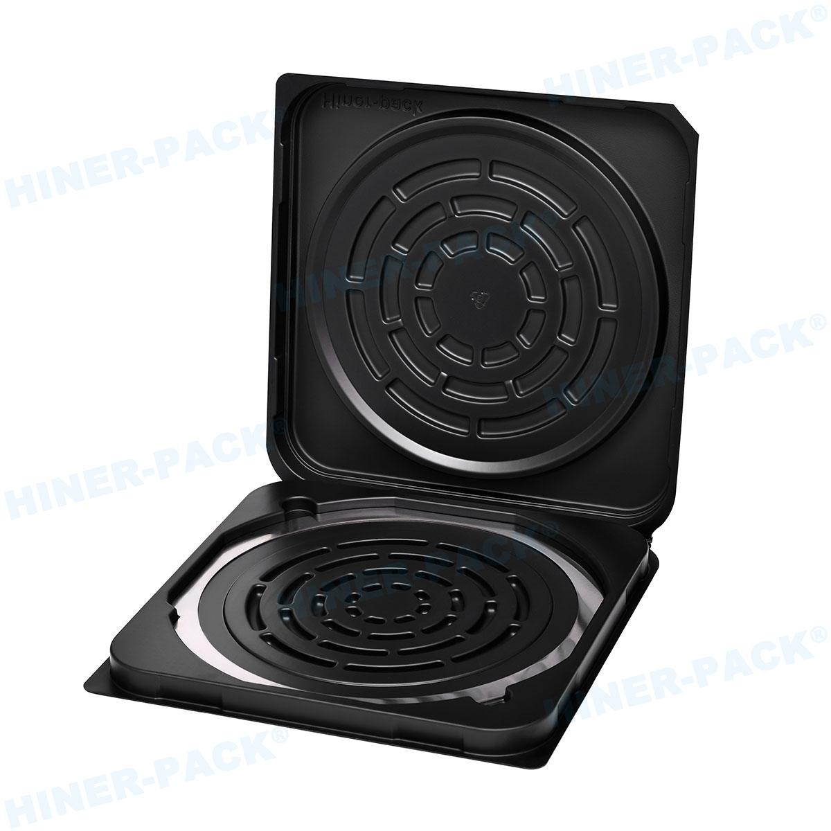
Main Body/Cassette: This is the primary structure that cradles the wafer. It features precisely spaced slots to hold the wafer securely at its edges, minimizing contact with the critical, active surface.
Door/Lid: The front-opening door creates a sealed environment. It often incorporates a sophisticated latching mechanism that ensures a secure closure during transport but allows for smooth, automated opening and closing by tool loadports.
RFID Tag and Memory: Modern single wafer box units are "intelligent." They are equipped with an embedded RFID tag that stores a unique identifier and vital information about the wafer's history, process steps, and specifications. This enables full traceability throughout the fab.
Gaskets and Seals: Critical for contamination control, these elastomeric components form a tight seal between the door and the body, preventing the ingress of external contaminants.
Handling Features: The box includes designed-in grips and alignment features for both human operators and robotic handlers, ensuring safe and precise transfer every time.
The Material Science Behind the Protection
You cannot just mold a single wafer box from any plastic. The materials used are subject to intense scrutiny and must meet extreme requirements.
Low Outgassing: The plastics must be exceptionally stable and release minimal volatile organic compounds (VOCs). Outgassed materials can condense on the wafer surface, creating defects during high-temperature process steps.
Static Dissipation: The buildup of static electricity can attract airborne particles like a magnet. Therefore, materials for a single wafer box are specially formulated to be static-dissipative, safely bleeding away any accumulated charge.
Chemical Resistance: The box must withstand repeated cleaning with aggressive chemicals and solvents without degrading, cracking, or leaching contaminants.
Dimensional Stability: The material must not warp or shrink over time or under varying temperature and humidity conditions. Maintaining precise slot positions is essential for robotic handling accuracy. Advanced thermoplastics like PEEK (Polyether Ether Ketone), PC (Polycarbonate) blends, and PPS (Polyphenylene Sulfide) are commonly used for their superior properties.
Seamless Integration with Automation and AMHS
Modern fabs are highly automated, dark environments where wafers are transported by robots and overhead hoists. The design of the single wafer box is intrinsically linked to this automated ecosystem.
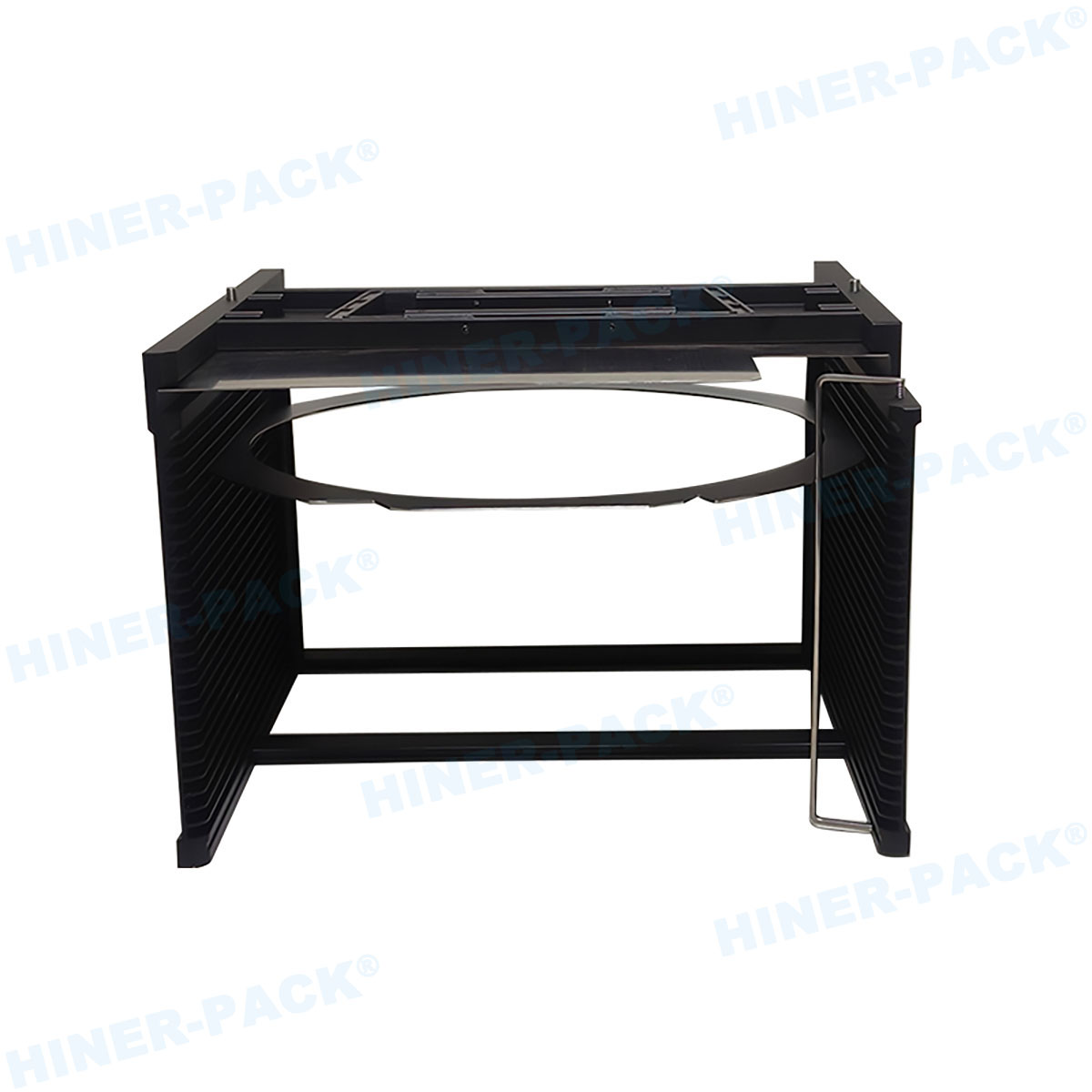
Standardized Footprint: Every single wafer box conforms to precise dimensional standards, allowing it to be seamlessly picked up, transported, and presented to the loadport of any processing tool.
Kinematic Coupling: The bottom of the box often features a kinematic mount—a set of precisely located grooves or pits. This mates with corresponding balls on the equipment loadport, ensuring highly repeatable and accurate positioning every time the box is placed down. This eliminates alignment errors that could lead to a wafer-handling crash.
Automated Door Engagement: The box's door is designed to be engaged by a mechanism on the tool's loadport. The robot never directly handles the delicate wafer; it simply moves the wafer from the secured, open box into the process chamber.
Ensuring Purity: Cleaning and Contamination Control Protocols
A single wafer box is a reusable asset. However, after each use, it must be returned to a state of ultra-cleanliness. The procedures for cleaning and maintaining these boxes are as critical as their initial design.
Specialized Cleaning Processes: Boxes undergo multi-stage cleaning in dedicated equipment using ultra-pure water, specialized chemicals, and megasonic energy to dislodge sub-micron particles.
Particle Monitoring: After cleaning, each single wafer box is rigorously inspected and tested for particle counts. Any unit that fails to meet the stringent cleanliness specifications (often allowing only a handful of particles per wafer slot) is rejected and re-cleaned or taken out of service.
Management of AMCs: Beyond particles, fabs are increasingly concerned with airborne molecular contaminants. Some advanced single wafer box designs incorporate materials or inner liners that actively absorb or neutralize specific AMCs, providing an extra layer of protection for sensitive processes.
Frequently Asked Questions (FAQ)
Q1: What is the main difference between a FOUP and a Single Wafer Box?
A1: A FOUP (Front Opening Unified Pod) is designed to carry a batch of multiple wafers (typically 13 or 25), while a single wafer box is dedicated to carrying one individual wafer. FOUPs are used for transporting wafers between tools within the same fab bay, whereas single wafer box carriers are more common for high-value wafers, engineering samples, or inter-fab transportation where individual tracking and maximum protection are required.
Q2: How many times can a single wafer box be reused?
A2: A high-quality single wafer box can be reused dozens, even hundreds, of times, provided it passes rigorous cleaning and inspection checks after every cycle. Its lifespan is determined by wear and tear on mechanical parts like the latch, the integrity of the seals, and whether it sustains any physical damage that compromises its cleanliness or dimensional stability.
Q3: Why is static control so important in a single wafer box?
A3: Static charge attracts particulate contamination like a magnet. If a single wafer box were made from static-prone materials, it would constantly draw airborne particles onto its surfaces and the wafer itself, leading to a high number of defects. Static-dissipative materials prevent this charge buildup, keeping the wafer surface clean.
Q4: Can a single wafer box be used for all wafer sizes?
A4: No. A single wafer box is designed for a specific wafer diameter, such as 200mm, 300mm, or the emerging 450mm standard. The design, internal dimensions, and handling features are all tailored to a precise wafer size to ensure a secure fit and proper interface with automated equipment.
Q5: What kind of data is stored on the RFID tag of a single wafer box?
A5: The RFID tag acts as the box's passport. It typically stores a unique ID, the wafer's identity, a history of process steps it has undergone, the wafer's specification (e.g., material, thickness), and sometimes cleaning and maintenance records for the box itself. This data enables full traceability, process control, and prevents misprocessing.


