In the fast-paced world of semiconductor manufacturing, precision and protection are paramount. One critical component that ensures the integrity of delicate wafers is the single wafer carrier box. This specialized container is designed to handle individual wafers during transport, storage, and processing, minimizing contamination and damage. As the industry shifts toward smaller nodes and higher yields, understanding the single wafer carrier box becomes crucial for professionals seeking to optimize their operations. In this article, we delve into five key aspects of the single wafer carrier box, providing insights that align with industry demands and search trends. Whether you're an engineer, a procurement specialist, or a tech enthusiast, this overview will highlight why the single wafer carrier box is indispensable in modern fabrication facilities.

What Is a Single Wafer Carrier Box?
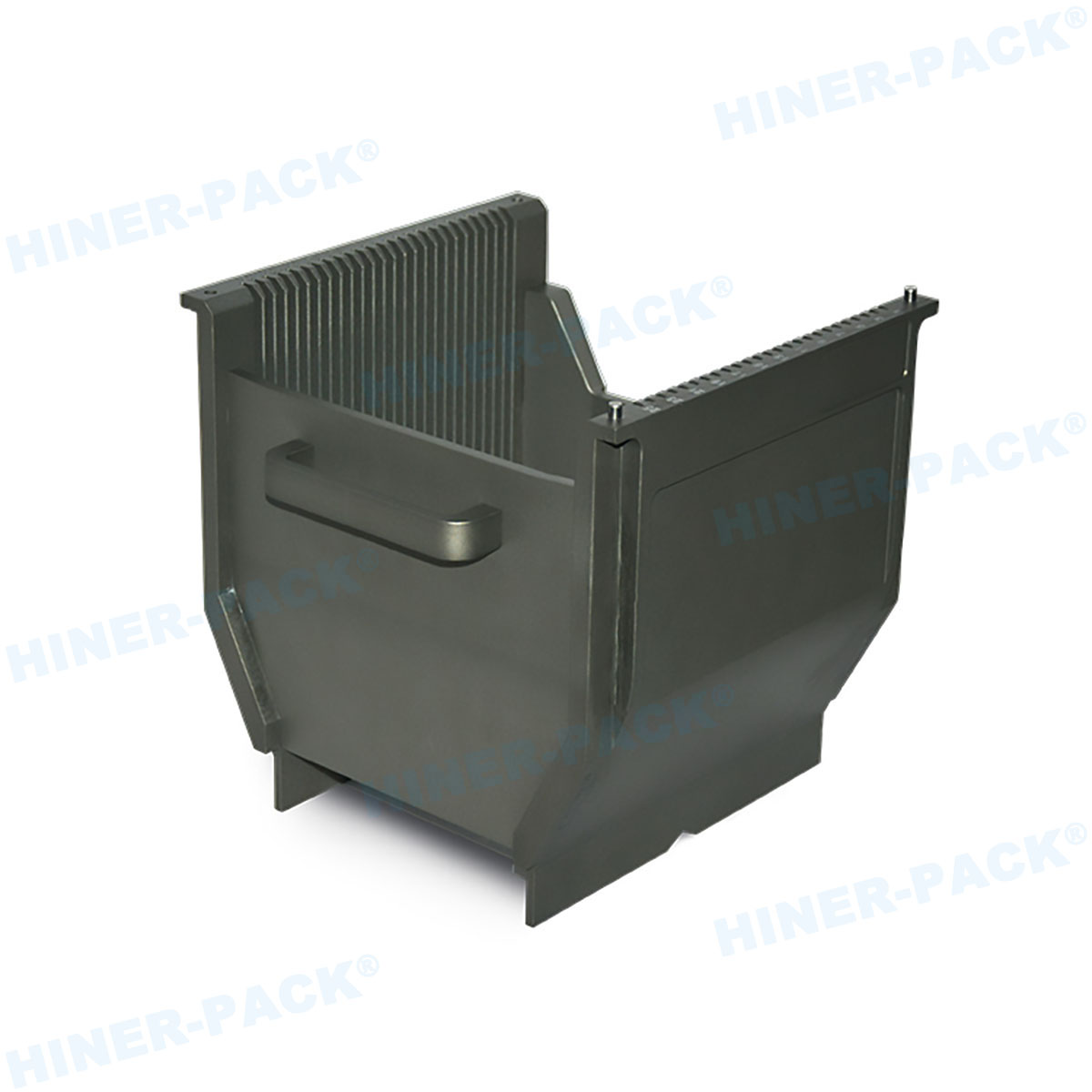
A single wafer carrier box is a protective enclosure specifically engineered to hold and safeguard individual semiconductor wafers. Unlike bulk carriers that handle multiple wafers, this single wafer carrier box isolates each wafer, reducing the risk of scratches, particles, and electrostatic discharge. Typically used in cleanroom environments, the single wafer carrier box is part of a broader ecosystem that includes front-opening unified pods (FOUPs) and standard mechanical interfaces (SMIF). The design of a single wafer carrier box focuses on compatibility with automated handling systems, ensuring seamless integration into production lines. By using a single wafer carrier box, manufacturers can maintain wafer purity from fabrication to assembly, which is vital for high-yield processes in industries like electronics and photovoltaics. The evolution of the single wafer carrier box has been driven by the need for higher precision in handling advanced materials, such as silicon and gallium arsenide wafers.
Design and Materials of Single Wafer Carrier Boxes
The design of a single wafer carrier box is a marvel of engineering, tailored to meet stringent industry standards. Most single wafer carrier boxes are constructed from high-purity polymers, such as polycarbonate or PEEK (polyether ether ketone), which offer excellent chemical resistance and low outgassing. These materials prevent contamination that could compromise wafer quality. The interior of a single wafer carrier box often features custom slots or cushions to cradle the wafer securely, while the exterior includes RFID tags or barcodes for tracking. Ventilation holes may be incorporated to allow for proper airflow during cleaning processes. Additionally, the single wafer carrier box is designed to be lightweight yet durable, capable of withstanding mechanical stress and temperature variations. Innovations in the single wafer carrier box design also include anti-static properties to dissipate charges, further protecting sensitive wafers. This attention to detail ensures that every single wafer carrier box performs reliably in demanding environments.
Key Benefits of Using Single Wafer Carrier Boxes
Adopting a single wafer carrier box brings numerous advantages to semiconductor manufacturing. First, it enhances wafer protection by minimizing contact and reducing particulate generation, which is critical for defect-free production. A single wafer carrier box also improves traceability, as each unit can be uniquely identified, streamlining inventory management. Moreover, the use of a single wafer carrier box supports faster processing times by enabling quick loading and unloading in automated systems. This efficiency translates to cost savings and higher throughput. Another benefit of the single wafer carrier box is its scalability; it can be easily integrated into existing workflows without major modifications. Compared to multi-wafer carriers, the single wafer carrier box reduces cross-contamination risks, making it ideal for high-mix, low-volume production. Overall, investing in a reliable single wafer carrier box can lead to improved yield rates and lower operational costs.
Applications in the Semiconductor Industry
The single wafer carrier box finds extensive applications across various stages of semiconductor manufacturing. In front-end processes, such as lithography and etching, the single wafer carrier box ensures that wafers remain uncontaminated during transfers between tools. Back-end operations, including dicing and packaging, also rely on the single wafer carrier box to maintain alignment and prevent damage. Beyond traditional IC fabrication, the single wafer carrier box is used in emerging fields like MEMS (Micro-Electro-Mechanical Systems) and LED production, where precision handling is essential. Research and development labs utilize the single wafer carrier box for prototyping and testing new materials, thanks to its versatility. As the industry embraces 5G and IoT technologies, the demand for the single wafer carrier box is expected to grow, driven by the need for higher reliability in complex device architectures.
Standards and Compliance for Single Wafer Carrier Boxes
Compliance with industry standards is a critical aspect of the single wafer carrier box. Organizations like SEMI (Semiconductor Equipment and Materials International) set guidelines for dimensions, materials, and performance. For instance, SEMI E142 specifies requirements for wafer carriers, including the single wafer carrier box, to ensure interoperability across different equipment. Adhering to these standards helps manufacturers avoid compatibility issues and reduces downtime. Additionally, the single wafer carrier box must meet cleanroom classifications, such as ISO 14644, which dictate particulate levels. Environmental regulations, like RoHS and REACH, also influence the materials used in a single wafer carrier box, promoting sustainability. Regular audits and certifications, such as ISO 9001, further validate the quality of a single wafer carrier box. By following these protocols, suppliers ensure that every single wafer carrier box delivers consistent performance and safety.
Maintenance and Cleaning Best Practices
Proper maintenance of a single wafer carrier box is essential for longevity and performance. Cleaning procedures typically involve automated systems that use deionized water, solvents, or plasma to remove contaminants. It's recommended to clean the single wafer carrier box after each use to prevent residue buildup. Inspection for cracks or wear should be part of routine checks, as defects can compromise wafer integrity. Storage of the single wafer carrier box in controlled environments, away from humidity and UV light, helps preserve its properties. Many facilities employ tracking software to monitor the lifecycle of each single wafer carrier box, scheduling replacements as needed. Training personnel on handling protocols, such as avoiding direct contact with interior surfaces, also plays a key role. By implementing these best practices, users can extend the service life of their single wafer carrier box and maintain high cleanliness standards.
In summary, the single wafer carrier box is a vital component in semiconductor manufacturing, offering unparalleled protection, efficiency, and compliance. From its innovative design to its diverse applications, the single wafer carrier box addresses the industry's need for precision and reliability. As technology advances, the role of the single wafer carrier box will only become more prominent, driving improvements in yield and cost-effectiveness. By understanding these aspects, professionals can make informed decisions that enhance their operations. Embrace the benefits of the single wafer carrier box to stay ahead in the competitive landscape of electronics production.
Frequently Asked Questions
Q1: What is the primary function of a single wafer carrier box?
A1: The primary function of a single wafer carrier box is to protect individual semiconductor wafers from physical damage, contamination, and electrostatic discharge during transport, storage, and processing in cleanroom environments.
Q2: How does a single wafer carrier box differ from multi-wafer carriers?
A2: Unlike multi-wafer carriers that hold several wafers together, a single wafer carrier box isolates each wafer, reducing the risk of cross-contamination and handling errors, which is crucial for high-precision applications.
Q3: What materials are commonly used in manufacturing a single wafer carrier box?
A3: Common materials for a single wafer carrier box include high-purity plastics like polycarbonate and PEEK, chosen for their low particulate generation, chemical resistance, and compliance with industry standards.
Q4: Can a single wafer carrier box be reused, and how should it be cleaned?
A4: Yes, a single wafer carrier box is often reusable. It should be cleaned using automated systems with deionized water or appropriate solvents, followed by inspections for damage to ensure it meets cleanliness specifications before reuse.
Q5: Are there specific standards that a single wafer carrier box must meet?
A5: Yes, a single wafer carrier box must adhere to standards such as SEMI E142 for dimensions and performance, along with cleanroom classifications like ISO 14644 and environmental regulations like RoHS to ensure safety and interoperability.


