In the pristine, hyper-controlled world of semiconductor fabrication, contamination is the enemy. While lithography scanners and etching tools capture the spotlight, the silent workhorses ensuring yield—wafer containers—are often an afterthought. This is a costly oversight.
Choosing the right wafer carrier is a direct investment in yield protection. A poor choice can introduce particles, cause mechanical damage, or lead to misprocessing, scrapping thousands of dollars worth of silicon in an instant. This isn't about buying a plastic box; it's about selecting a precision component integral to your process stability.
Let’s break down the five non-negotiable factors for evaluating wafer shipping boxes and process carriers. We’ll also touch on why suppliers with deep material science expertise, like Hiner-pack, are becoming essential partners for fabs focused on pushing advanced nodes.
1. Function Dictates Form: Understanding Wafer Container Types
Not all wafer containers serve the same purpose. Using the wrong type for a given step is a fundamental error. The industry has standardized around a few key designs:
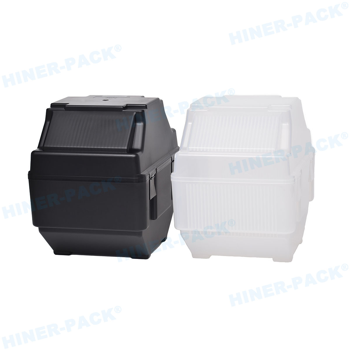
FOUPs (Front-Opening Unified Pods): The absolute standard for automated 300mm wafer processing. These sealed pods maintain a mini-environment (often filled with inert gas) and interface directly with tool loadports. They are for in-fab, in-tool use.
FOSBs (Front-Opening Shipping Boxes): Designed for 300mm wafer transport and storage outside the tool environment. They protect wafers but are not hermetically sealed like FOUPs. Wafers are typically transferred from a FOSB to a FOUP at the tool.
SMIF Pods (Standard Mechanical Interface): The predecessor to FOUPs, still widely used for 200mm and smaller wafers. They provide a similar mini-environment function for automated lines.
Open Cassettes: Simple, open carriers for manual handling or transport within a specific process bay. They offer minimal environmental isolation.
Rigid Wafer Shipping Boxes: Heavy-duty, crush-resistant containers with robust sealing for inter-factory or international transport. They must withstand logistics hazards like vibration and humidity swings.
Selecting the correct type is step one. A FOSB cannot replace a FOUP at the tool interface, and an open cassette is never suitable for long-term storage.
2. The Material Science: More Than Just "Plastic"
The resin used in your wafer carrier is a critical variable. It must achieve a near-impossible balance: be incredibly pure, chemically inert, dimensionally stable, and mechanically tough.
PBT (Polybutylene Terephthalate): A workhorse material. It offers a good balance of low particle generation, chemical resistance, and cost for many process steps.
PFA (Perfluoroalkoxy alkane): The high-purity champion. Used for the most sensitive processes and wet benches, PFA offers virtually no ionic contamination and outstanding resistance to aggressive chemicals. It’s more expensive but often necessary.
Carbon-Filled Plastics: Essential for ESD (Electrostatic Discharge) protection. Dissipative or conductive materials prevent charge buildup that can zap delicate circuits on the wafer.
The wrong material will degrade, shed particles, or leach contaminants. Leading manufacturers, including Hiner-pack, don't just mold plastic; they engineer with specific, certified polymers for defined applications, understanding how each resin behaves through hundreds of clean and process cycles.
3. The Hidden Enemies: Particles, ESD, and Outgassing
A wafer container’s primary job is defense. You must evaluate its performance against three key threats:
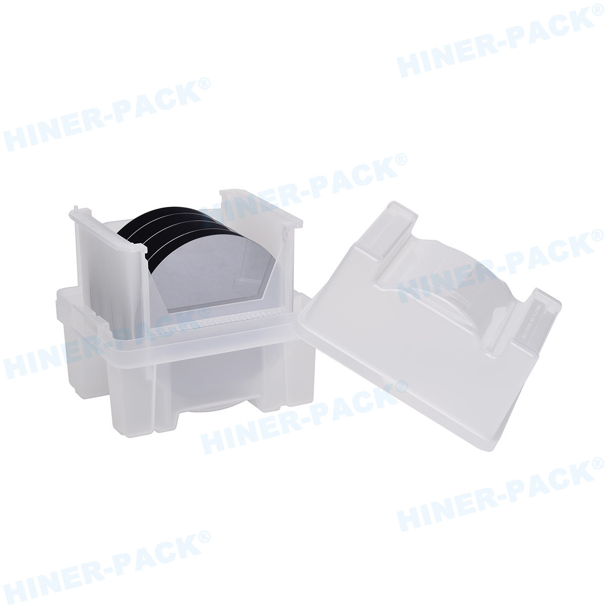
Particle Control: Every surface must be designed to minimize generation and adhesion. This includes slot design, smooth interior geometries, and advanced polymer formulations. Particle counts are measured in the single digits per wafer pass.
ESD Protection: As feature sizes shrink, ESD sensitivity skyrockets. Wafer shipping boxes and carriers must have controlled resistivity to safely ground any static charge without being so conductive they cause shorting.
Outgassing: The container must not release (outgas) volatile organic compounds into its enclosed environment. These compounds can deposit on wafer surfaces, creating defects. Low outgassing is a hallmark of high-grade materials.
Your container is your wafer’s mobile cleanroom. Its defensive specs must match or exceed the cleanliness class of your fab.
4. Compatibility and Handling: The Integration Factor
A perfect wafer box is useless if it doesn’t integrate seamlessly. Compatibility is multifaceted:
Tool Compatibility: Does it meet the exact physical and kinematic dimensions for your specific AMHS (Automated Material Handling System) and tool loadports? Even a millimeter of deviation can cause a jam.
Wafer Size Compatibility: 200mm, 300mm, and emerging sizes require dedicated, non-interchangeable wafer containers. Ensure the carrier is designed for your wafer diameter and thickness profile.
Process Compatibility: Is it clean enough for your most sensitive lithography step? Chemically resistant enough for your wet etch area? One size rarely fits all.
Furthermore, consider ergonomics and handling. Even in automated fabs, manual handling occurs. Designs that facilitate safe, easy access without wafer contact reduce risk.
5. Total Cost of Ownership: Looking Beyond the Price Tag
The cheapest wafer container is often the most expensive. Total Cost of Ownership (TCO) includes:
Initial Purchase Price: The obvious starting point.
Cleaning & Maintenance Cost: How often must it be cleaned? How durable is it through cleaning cycles? Carriers that degrade quickly increase lifetime costs.
Yield Impact: This is the massive variable. A single particle event causing a tool downtime or batch loss can eclipse the cost of thousands of premium carriers. Reliability is a yield driver.
Replacement Cycle: High-quality wafer carriers from trusted suppliers maintain their specs longer, delaying capital refresh cycles.
Investing in robust, reliable wafer shipping boxes and process carriers is a proactive strategy for yield protection. It’s an area where corner-cutting manifests directly on the bottom line as reduced output and increased scrap.
An Engineered Component, Not a Commodity
Wafer containers are precision-engineered components that directly influence manufacturing success. The selection process should be as rigorous as for any piece of process equipment.
By focusing on the type, material, protective performance, compatibility, and true lifetime cost, fabs can make informed decisions that safeguard their most valuable asset—the silicon wafer. Partnering with specialized manufacturers who provide technical data, material traceability, and consistent quality, such as Hiner-pack, is no longer a luxury but a necessity for competitive manufacturing at advanced technology nodes.
Frequently Asked Questions (FAQs)
Q1: What is the real difference between a FOUP and a wafer shipping box?
A1: A FOUP is designed for in-tool processing in an automated 300mm fab. It’s part of the tool's mini-environment. A wafer shipping box (like a rigid sealed container) is built for physical transportation between facilities, focusing on crush resistance and hermetic sealing against external environmental hazards.
Q2: How can I tell if my current wafer containers are failing?
A2: Key signs include a measurable increase in particle counts on monitor wafers, visible wear or scratches on the container's interior slots, difficulty with robotic insertion/retrieval, and increased ESD events. Regular monitoring and scheduled preventative replacement are crucial.
Q3: Are there "universal" wafer containers that work for both 200mm and 300mm wafers?
A3: No. The physical standards for 200mm (SMIF) and 300mm (FOUP/FOSB) wafer containers are completely different and incompatible. They have different footprints, docking mechanisms, and handling protocols. Using the correct, size-specific carrier is mandatory.
Q4: Why can't we use metal containers for better durability?
A4: Metals are generally avoided for direct wafer contact due to risks of ionic contamination, particle generation from metal-on-metal contact, and the potential for creating shorts or interfering with processes. High-purity, engineered plastics and fluoropolymers offer the necessary cleanliness and chemical inertness.
Q5: When should I consider a specialized material like PFA over standard PBT for a carrier?
A5: Specify PFA or other high-end fluoropolymers when the wafers will be exposed to aggressive chemistries (e.g., in wet benches), for extremely high-temperature processes, or for the most critical process steps at advanced nodes (e.g., post-lithography storage) where the absolute lowest risk of ionic or organic contamination is required.


