The semiconductor manufacturing process is an unforgiving environment. A microscopic speck of dust or a minor electrostatic discharge can destroy a wafer worth tens of thousands of dollars. In this high-stakes setting, the humble plastic containers used to transport silicon disks are not just boxes; they are critical engineering tools.
Moving wafers between process steps, from lithography to etching, and eventually to shipping, requires specialized equipment. This is where wafer carriers become the unsung heroes of fabrication plants (fabs). They protect delicate substrates from physical damage, contamination, and chemical exposure.
For procurement managers and process engineers, selecting the right carrier is about balancing material properties, automation compatibility, and cost. Industry providers like Hiner-pack have observed that as node sizes shrink, the precision required for these carriers increases significantly.
The Role of Wafer Carriers in Modern Fabs
At its core, a carrier is designed to hold silicon wafers securely. However, the function goes far beyond simple storage. Modern fabs rely on Automated Material Handling Systems (AMHS). Robots and overhead hoist transports (OHT) move wafers at high speeds.
If a carrier is slightly warped or does not meet precise dimensional standards, the robotic interface can fail. This leads to downtime or, worse, wafer breakage. Therefore, the mechanical stability of these containers is paramount.
Carriers also serve as micro-environments. Once a pod is sealed, it must maintain a specific atmosphere, often nitrogen-purged, to prevent oxidation on the wafer surface. This effectively isolates the silicon from the cleanroom air, which—despite being clean—might still contain molecular contaminants.
Key Materials: Beyond Standard Plastics
You cannot use standard plastic in a cleanroom. The materials used for manufacturing wafer carriers must possess specific characteristics to ensure high yield.
PEEK (Polyether ether ketone)This is the gold standard for high-temperature and harsh chemical applications. PEEK offers excellent dimensional stability and low outgassing. It is often used for process cassettes that go into cleaning baths or hot environments.
PFA (Perfluoroalkoxy)PFA is highly resistant to strong acids and solvents. In wet etch processes where aggressive chemicals are used to strip layers off the silicon, PFA carriers are necessary because they will not degrade or leach contaminants into the bath.
Polypropylene (PP) and Polycarbonate (PC)These materials are typically used for storage and shipping boxes where extreme chemical resistance isn't the primary concern. They are cost-effective and durable. However, manufacturers usually add carbon powder or fibers to these plastics to create ESD (Electrostatic Discharge) safe variants.
Understanding Electrostatic Discharge (ESD)
Static electricity is a silent killer in the semiconductor industry. As wafers move against the slots of a carrier, friction can generate a charge. If this charge discharges into the circuit, it can fuse microscopic gates and destroy the chip.
High-quality carriers utilize electrostatic dissipative materials. These materials allow the charge to bleed off slowly and safely to the ground rather than sparking. When evaluating suppliers, ensuring their materials meet ANSI/ESD standards is a non-negotiable step.
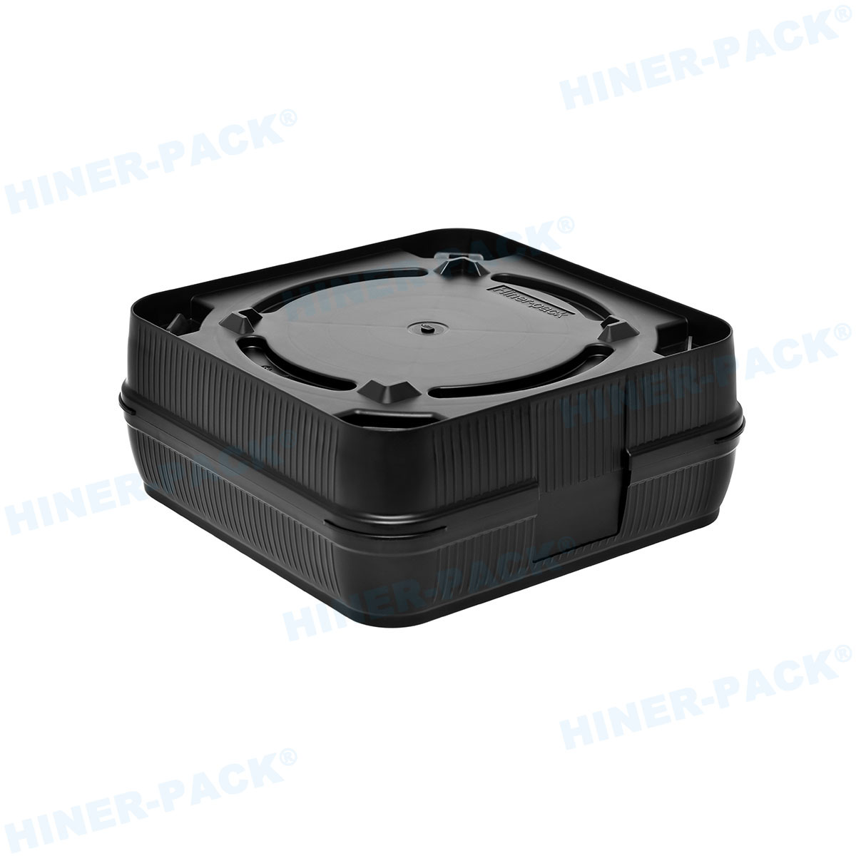
Front Opening Unified Pods (FOUPs)
In the era of 300mm (12-inch) wafers, the FOUP is the standard carrier. Unlike the open cassettes used in older 200mm fabs, FOUPs are fully enclosed environments.
A FOUP holds up to 25 wafers. It features a front door that is designed to be opened only by the process tool. When a FOUP is docked, the tool opens the door, slides the wafers out, processes them, and returns them, all without exposing the silicon to the external cleanroom environment.
The mechanical interface of a FOUP is complex. It uses kinematic coupling pins on the bottom to ensure perfect alignment with the tool. Even a millimeter of deviation can cause a handler error.
Front Opening Shipping Boxes (FOSBs)
While a FOUP is used inside the fab, a FOSB is used to move wafers between facilities. For example, moving wafers from the fab where they are made to the assembly and test facility where they are diced and packaged.
FOSBs look similar to FOUPs but are generally simpler in design. They prioritize shock absorption and vibration resistance during truck or air transport. They typically do not require the high-precision robotic interfaces needed for process tools, making them more cost-effective for logistics.
Process Cassettes and Boats
For 150mm and 200mm lines, or for specific batch processes in 300mm lines, open cassettes are still widely used. These "boats" hold wafers upright and are dipped directly into chemical tanks or placed into furnaces.
Quartz and Silicon Carbide are often used for furnace boats due to extreme heat, but for wet processes, fluoropolymers are preferred. The design of the slot is critical here. It must minimize contact with the wafer edge to reduce "shadowing" during cleaning processes, where the carrier might block the chemical spray.
Coin Stack and Horizontal Shippers
Not all wafer carriers keep wafers separated vertically. For shipping finished wafers or thinner substrates, horizontal shippers (often called coin stack containers) are common.
In this configuration, wafers are stacked directly on top of each other with interleaf paper or foam separators in between. This density allows for shipping hundreds of wafers in a small footprint. However, this is generally reserved for finished wafers that have a protective passivation layer, as the face-to-face contact could damage sensitive circuits on work-in-progress wafers.
The Importance of Cleaning and Maintenance
Carriers are not single-use items. They are expensive assets that are cycled through the fab thousands of times. Over time, they accumulate particles and chemical residues.
Fabs have dedicated carrier cleaning systems. These wash stations use surfactants and DI water to strip contaminants from the plastic. However, repeated washing can degrade the material.
A worn-out carrier might warp, leading to cross-threading of the robotic screws or failure to seal properly. Regular inspection of the carrier fleet is a standard operating procedure. Brands like Hiner-pack often provide guidelines on the expected lifecycle of their products to help fabs plan for replacements before failures occur.
Automation and The "Human" Factor
Despite the heavy automation, human operators still handle carriers, especially during transport between older tools or during shipping preparation. Ergonomics plays a role here.
Handles must be designed to be gripped easily by operators wearing thick cleanroom gloves. The weight of a fully loaded 300mm carrier is significant (often over 9kg). Poor ergonomic design can lead to drops, which is a catastrophic event in a fab. A dropped carrier doesn't just mean broken silicon; it means shutting down that area of the cleanroom to clean up hazardous shards.
Outgassing: The Invisible Threat
One of the most insidious problems in wafer storage is outgassing. Plastics, over time, can release volatile organic compounds (VOCs). If a wafer sits in a closed carrier for weeks, these VOCs can condense on the wafer surface, creating a haze.
This organic haze can interfere with sensitive lithography steps or cause delamination in packaging. High-purity materials are formulated specifically to have low outgassing properties. When storing wafers for long periods, fabs often use purge-capable carriers that constantly cycle nitrogen through the box to sweep away any outgassed molecules.
Supply Chain Security
The semiconductor shortage of recent years highlighted the fragility of the supply chain. This extends to consumables like wafer carriers. If a fab runs out of FOSBs, they cannot ship their product to customers.
Diversifying suppliers is a strategy many procurement departments are adopting. Relying on a single source for critical plastics is risky. Evaluating the production capacity and lead times of different vendors is just as important as technical specifications.
Shipping Finished Wafers
Once the fabrication is complete, the wafers are thinned and prepared for dicing. Thin wafers are incredibly fragile. Special carriers with frame support (tape rings) are used here.
These carriers hold the metal ring that stretches the dicing tape. The wafer is mounted on the tape. The carrier must support the metal ring rigidly while ensuring nothing touches the fragile wafer surface.
Trends in Carrier Technology
As the industry moves toward heterogeneous integration and advanced packaging, the types of substrates are changing. Glass carriers and bonded wafers are becoming more common.
Standard carriers often don't fit these new form factors. Customization is becoming a key requirement. Suppliers who can rapidly prototype and mold new carrier designs are in high demand.
Furthermore, the push for sustainability is reaching the cleanroom. Fabs are looking for recycling programs for end-of-life carriers. While recycling contaminated plastics is difficult, grinding down non-hazardous shipping boxes for re-extrusion into lower-tier products is a growing trend.
Selecting the Right Vendor
When choosing a partner for wafer handling, look for transparency in data. A good vendor should provide detailed reports on particle generation, ionic contamination, and discharge times for ESD materials.
It is also beneficial to work with companies that have a broad portfolio. A supplier that offers both in-fab process cassettes and outbound shipping boxes can offer better volume pricing and consistent quality control. Hiner-pack is an example of a brand that covers multiple aspects of this ecosystem, providing options that cater to both legacy nodes and cutting-edge processes.
The yield of a semiconductor fab is directly tied to how well it protects its wafers during transport. Wafer carriers are the first line of defense against the chaotic world outside the cleanroom. From the material science of PEEK and PFA to the mechanical precision of a FOUP’s docking interface, every detail matters.
Ignoring the quality of these containers is a costly mistake. By investing in high-quality, ESD-safe, and dimensionally stable carriers, manufacturers ensure that their valuable silicon makes it from the ingot to the final device without defect. Whether you are setting up a new line or optimizing an existing one, reviewing your carrier strategy with trusted partners like Hiner-pack can lead to measurable improvements in operational efficiency and product yield.
Common Questions (FAQ)
Q1: What is the main difference between a FOUP and a FOSB?
A1: A FOUP (Front Opening Unified Pod) is designed for internal use within the fab. It has high-precision interfaces for robotic tools and supports automated processing. A FOSB (Front Opening Shipping Box) is designed for transporting wafers between different facilities (e.g., from fab to assembly). FOSBs prioritize impact resistance and secure wafer retention during shipping rather than robotic precision.
Q2: Why are PEEK materials preferred for certain wafer carriers?
A2: PEEK is chosen for its exceptional thermal and chemical resistance. It can withstand high temperatures and aggressive chemicals used in cleaning and etching processes without deforming or releasing contaminants. It also maintains its shape (dimensional stability) better than most plastics, which is critical for automation.
Q3: How do you prevent static damage when using plastic carriers?
A3: Standard plastics are insulators and generate static. To prevent this, wafer carriers are made from ESD (Electrostatic Discharge) safe materials. Manufacturers add carbon fiber or carbon powder to the polymer mix. This makes the plastic slightly conductive, allowing static charges to dissipate safely to the ground rather than arcing to the wafer.
Q4: Can wafer carriers be cleaned and reused?
A4: Yes, most process carriers and shipping boxes are designed to be reusable. Fabs use specialized carrier wash stations that clean the boxes with deionized water and detergents. However, they have a finite lifespan. Over time, the material may degrade or warp, requiring replacement to ensure they don't cause robot errors.
Q5: What are the standard sizes for wafer carriers?
A5: Carriers are sized according to the wafer diameter. The most common standard sizes are for 150mm (6-inch), 200mm (8-inch), and 300mm (12-inch) wafers. There are also carriers for smaller sizes like 100mm used in research or compound semiconductors (like GaN or SiC). The industry has strict SEMI standards ensuring carriers from different vendors fit the same processing tools.


