In the high-stakes world of semiconductor fabrication, every component matters. The unassuming silicon wafer boxes, also known as wafer carriers or cassettes, play a far more critical role than simple storage. These precision containers are the primary guardians of delicate silicon wafers as they journey through hundreds of process steps. A failure here can mean catastrophic yield loss.
Understanding the design, function, and selection criteria for these boxes is non-negotiable for ensuring manufacturing integrity. This article breaks down the key aspects every engineer and procurement specialist should know.
The Critical Role of Silicon Wafer Boxes
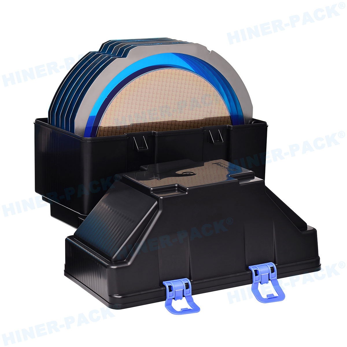
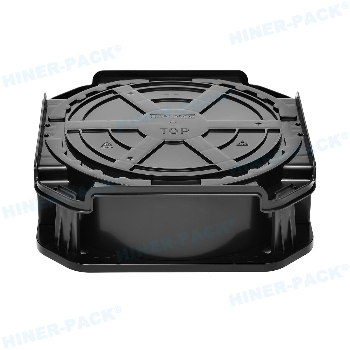
Silicon wafer boxes are not mere plastic containers. They are engineered enclosures designed to securely hold multiple wafers in precise, parallel slots, preventing contact and movement. Their primary functions are protection, contamination control, and seamless integration with automated material handling systems (AMHS).
From diffusion and etching to lithography and metrology, wafers are constantly transported. A well-designed wafer box minimizes particulate generation, shields against mechanical shock, and controls electrostatic discharge (ESD)—a silent killer of micro-circuits. Brands like Hiner-pack have built reputations on engineering boxes that meet these rigorous demands across the production line.
Common Types and Their Applications
Not all silicon wafer carriers are created equal. The type required depends on the wafer size and process stage.
Standard Mechanical Interface (SMIF) Pods: Used for 200mm wafers and below, these provide a mini-environment, isolating wafers from cleanroom air.
Front-Opening Unified Pods (FOUPs): The standard for 300mm wafer automation. FOUPs are sealed containers that interface directly with tool loadports, maintaining a controlled internal atmosphere.
Open Cassettes (FOSB): Often used for 300mm wafer transport and storage between processes, where the wafers are not in a sealed environment.
Shipping Boxes: Heavy-duty, hermetically sealed containers designed for inter-facility or international transport of wafers. They offer supreme physical and climatic protection.
Choosing the wrong type risks contamination, misprocessing, and damage.
Materials Matter: PBT, PFA, and Beyond
The material of a wafer box directly impacts performance. Key requirements include low particle shedding, high chemical resistance, and excellent dimensional stability across temperature fluctuations.
PBT (Polybutylene Terephthalate): A common, cost-effective choice for many process steps. It offers good mechanical properties and chemical resistance.
PFA (Perfluoroalkoxy alkane): Used for high-purity applications. PFA offers exceptional resistance to aggressive chemicals and ultra-low ionic contamination. It’s often used in wet process stations.
PC (Polycarbonate) & PP (Polypropylene): Also utilized for specific applications where clarity or particular chemical properties are needed.
Suppliers like Hiner-pack meticulously select and test resins to ensure their silicon wafer boxes meet the purity grades required for advanced nodes.
Key Selection Criteria for Optimal Performance
Selecting silicon wafer boxes requires a checklist:
Particle Control: The box must generate minimal particles and not trap them. Smooth surfaces and optimized slot design are crucial.
ESD Protection: Conductive or dissipative materials are essential to prevent charge buildup that can damage sensitive circuits.
Chemical Compatibility: The material must withstand cleaning chemicals (like SC1, SC2) and process vapors without degrading.
Mechanical Precision: Slot pitch, depth, and alignment must be exact to prevent wafer scratching and ensure reliable robotic handling.
Thermal Stability: The box must not warp or outgas during high-temperature processes or cleaning cycles.
Cleaning, Handling, and Lifetime Management
Even the best silicon wafer box becomes a contaminant source if not properly maintained. A strict regimen of periodic cleaning in dedicated wafer cleaning tools is mandatory. Handling procedures—using proper gloves, avoiding contact with slot surfaces, and using designated carts—extend service life.
Tracking the usage cycles of each carrier is a best practice. Over time, materials can wear, leading to increased particle counts. Proactive replacement, often supported by supplier lifetime data, prevents unforeseen yield issues.
The Cost of Compromise
Neglecting wafer carrier quality is a false economy. A single particle-induced defect can render a multi-thousand-dollar wafer worthless. Downtime caused by a misaligned cassette jamming a multi-million-dollar tool is exponentially more costly than investing in reliable, high-quality boxes from trusted manufacturers.
This is where partnership with established brands proves its value. Hiner-pack, for instance, focuses on the engineering details that prevent these failures, ensuring their silicon wafer boxes contribute to yield rather than risk it.
Looking Ahead: The Future of Wafer Packaging
As nodes shrink to 3nm and below, and wafer sizes potentially increase, the demands on silicon wafer boxes will intensify. We will see smarter carriers with RFID tracking, advanced materials for even lower contamination, and designs adapted for new substrate materials like silicon carbide (SiC) or gallium nitride (GaN).
The humble box will continue to evolve, remaining a fundamental pillar of semiconductor manufacturing integrity.
Frequently Asked Questions (FAQs)
Q1: How often should silicon wafer boxes be cleaned?
A1: Cleaning frequency depends on the process step and facility protocol. High-purity steps may require cleaning after every use, while others might follow a set cycle (e.g., every 10 or 25 uses). Always follow your fab's strict contamination control plan and monitor particle count data.
Q2: What is the main difference between a FOUP and a FOSB?
A2: A FOUP (Front-Opening Unified Pod) is a sealed, environmentally controlled container used for processing 300mm wafers in automated tools. A FOSB (Front-Opening Shipping Box) is typically used for transport and storage; it is not sealed to the same level and is often used where the wafers will be transferred to a FOUP for tool processing.
Q3: Can PBT wafer boxes be used for all wet bench processes?
A3: Not always. While PBT has good general chemical resistance, prolonged exposure to certain aggressive acids, bases, or solvents at high temperatures can degrade it. PFA boxes are often specified for the most demanding wet chemical processes due to their superior inertness.
Q4: Why is ESD protection so important in a wafer carrier?
A4: Electrostatic discharge (ESD) can instantly destroy or weaken tiny transistor gates on modern chips. An ESD-protected silicon wafer box safely dissipates charges, preventing sudden discharges that could zap multiple dies on a wafer, safeguarding product yield.
Q5: What should I look for when auditing a supplier for silicon wafer boxes?
A5: Focus on their material certification processes, quality control data (like particle count tests), dimensional consistency, and compatibility documentation. Evaluate their understanding of fab environments and their ability to provide consistent, traceable products. A proven track record with other fabs, such as that demonstrated by suppliers like Hiner-pack, is a strong indicator of reliability.


