5 Critical OEM Wafer Shipping Solutions for Global Semiconductor Supply ChainsThe semiconductor industry relies on precise and secure logistics to transport delicate wafers. Effective OEM wafer shipping solutions are essential for minimizing damage and maintaining supply chain integrity. Companies like Hiner-pack provide specialized products to meet these demands, ensuring wafers reach their destination safely.
Why Reliable OEM Wafer Shipping Solutions Matter
In semiconductor manufacturing, wafers are highly sensitive to physical and environmental stresses. Any mishandling during transit can lead to costly defects and production delays. Robust OEM wafer shipping solutions address these risks by offering tailored protection and logistics support.
Protecting Delicate Wafers During Transit
Wafers, especially those with advanced nodes, require careful handling. Shipping solutions must prevent contamination, shock, and vibration.
Use of static-controlled materials to avoid electrostatic discharge.
Shock-absorbing designs to cushion against impacts.
Sealed environments to keep out dust and moisture.
Ensuring Supply Chain Efficiency
Efficient logistics reduce transit times and costs. OEM solutions streamline processes from fabrication to assembly sites.
Standardized packaging for easy integration into automated systems.
Lightweight designs to lower shipping expenses.
Compatibility with global shipping regulations and methods.
Key Components of Effective OEM Wafer Shipping Solutions
Successful shipping relies on several core elements. Each component plays a role in safeguarding wafers and optimizing logistics.
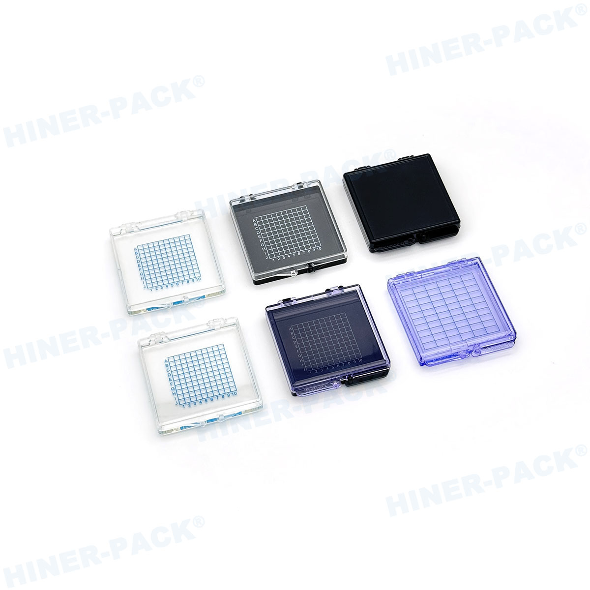
Wafer Shippers and Carriers
These are primary containers that hold wafers securely. They come in various sizes and materials to match specific needs.
Rigid plastic shippers for durability and reusability.
Foam inserts for added cushioning and wafer separation.
Stackable designs to maximize space during storage and transport.
Accessories and Cushioning Materials
Additional items enhance protection and functionality. They include liners, dividers, and labeling systems.
Antistatic bags to prevent charge buildup.
Custom foam cutouts for irregular wafer shapes.
Barcodes and RFID tags for tracking and inventory management.
Customization in OEM Wafer Shipping Solutions
Every semiconductor project has unique requirements. Customized solutions ensure that wafers are handled according to specific standards and conditions.
Tailored Solutions for Different Wafer Sizes
Wafers range from 150mm to 300mm or larger. Shipping containers must be sized accurately to avoid movement and damage.
Adjustable carriers for multiple wafer diameters.
Special designs for thin wafers or those with coatings.
Temperature-controlled options for sensitive materials.
Branding and Identification
Clear identification helps in logistics and inventory control. Custom branding can include company logos and color coding.
Printed labels with part numbers and handling instructions.
Color-coded lids for quick recognition of wafer types.
Integration with factory automation systems for seamless processing.
Compliance and Standards in OEM Wafer Shipping Solutions
International standards govern wafer shipping to ensure safety and quality. Compliance is critical for global trade and industry acceptance.
International Standards
Organizations like SEMI set guidelines for wafer packaging and shipping. Adhering to these standards reduces risks and fosters trust.
SEMI standards for materials, dimensions, and performance.
ISO certifications for quality management systems.
Regulations on hazardous materials and environmental impact.

Environmental Considerations
Sustainability is becoming important in semiconductor logistics. Eco-friendly materials and designs help reduce waste.
Reusable shipping containers to minimize disposable waste.
Recyclable plastics and foams in construction.
Energy-efficient manufacturing processes for shipping products.
Hiner-pack's Role in OEM Wafer Shipping Solutions
Hiner-pack is a trusted provider of specialized shipping products for the semiconductor industry. Their offerings align with the needs of modern wafer logistics.
They focus on durability, customization, and compliance. Products include wafer shippers, carriers, and accessories designed for global supply chains.
High-quality materials that meet SEMI standards.
Custom designs for OEM clients to fit specific workflows.
Global distribution support to ensure timely delivery.
By partnering with Hiner-pack, companies can enhance their OEM wafer shipping solutions for better reliability and efficiency.
Effective logistics are vital for the semiconductor industry. Implementing robust OEM wafer shipping solutions helps protect wafers, streamline supply chains, and meet international standards. With providers like Hiner-pack, manufacturers can achieve safer and more cost-effective transport.
Frequently Asked Questions (FAQ)
Q1: What are OEM wafer shipping solutions?
A1: OEM wafer shipping solutions refer to customized packaging and logistics systems designed for transporting semiconductor wafers. They include containers, accessories, and services that protect wafers from damage during transit.
Q2: Why is customization important in wafer shipping?
A2: Customization ensures that shipping solutions fit specific wafer sizes, materials, and handling requirements. It enhances protection, improves efficiency, and supports integration into existing production lines.
Q3: What standards apply to OEM wafer shipping solutions?
A3: Key standards include SEMI guidelines for packaging and ISO certifications for quality. Compliance with these standards ensures safety, reliability, and global acceptance in the semiconductor industry.
Q4: How do Hiner-pack's products support wafer shipping?
A4: Hiner-pack offers durable wafer shippers, carriers, and accessories that meet industry standards. Their products are customizable and designed to safeguard wafers, contributing to effective OEM wafer shipping solutions.
Q5: Can OEM wafer shipping solutions reduce costs?
A5: Yes, by minimizing wafer damage and optimizing logistics, these solutions can lower replacement costs and shipping expenses. Reusable designs and efficient packaging also contribute to long-term savings.