
In the high-stakes world of semiconductor manufacturing, the journey doesn't end at the fab. Protecting the delicate, patterned silicon wafers during transit, storage, and handling is paramount. A single impact can render millions of dollars in R&D and production worthless. This is where impact resistant wafer packaging transitions from a simple logistical box to a critical component of the supply chain.
This guide delves into the five key innovations revolutionizing how the industry safeguards its most valuable assets. We will explore the technologies, compare solutions, and provide a selection guide to ensure your wafers arrive flawlessly.
Why Impact Resistance is Non-Negotiable in Modern Fabs
Semiconductor nodes continue to shrink, with 3nm and 2nm processes becoming mainstream. Wafers for these technologies are incredibly thin and fragile. Traditional packaging might protect against dust and minor scratches, but it is often insufficient against the shocks and drops inherent in global logistics.
The cost of wafer breakage or micro-cracking is astronomical. It leads to:
Direct financial loss.
Production delays.
Compromised end-product reliability.
Impact resistant wafer packaging is engineered to absorb and dissipate kinetic energy, preventing it from reaching the wafer inside. It's your first and most crucial line of defense.
The Evolution from Standard to High-Performance Solutions
Historically, wafer shippers were simple plastic or metal containers with foam inserts. While functional for older, thicker wafers, they lack the sophisticated engineering needed today.
Modern impact resistant wafer packaging solutions are a feat of material science and structural design. They have evolved to address:
Higher G-Forces: Certified to withstand specific drop heights.
Contamination Control: Made from low-outgassing, ultra-clean materials.
Static Dissipation: Critical for protecting sensitive circuits.
Weight Optimization: Reducing shipping costs without compromising protection.
Core Technologies Behind Superior Impact Protection
What makes one wafer shipper more protective than another? It boils down to three core technological areas.
1. Advanced Cushioning Materials
Gone are the days of simple foam. Today's solutions use multi-layer, engineered polymers and composite foams. These materials are designed to have a specific crush strength, allowing them to deform predictably under impact, absorbing energy and then returning to their original shape.
Customized foam formulations can be created for specific wafer sizes and fragility levels, a service Hiner-pack specializes in.
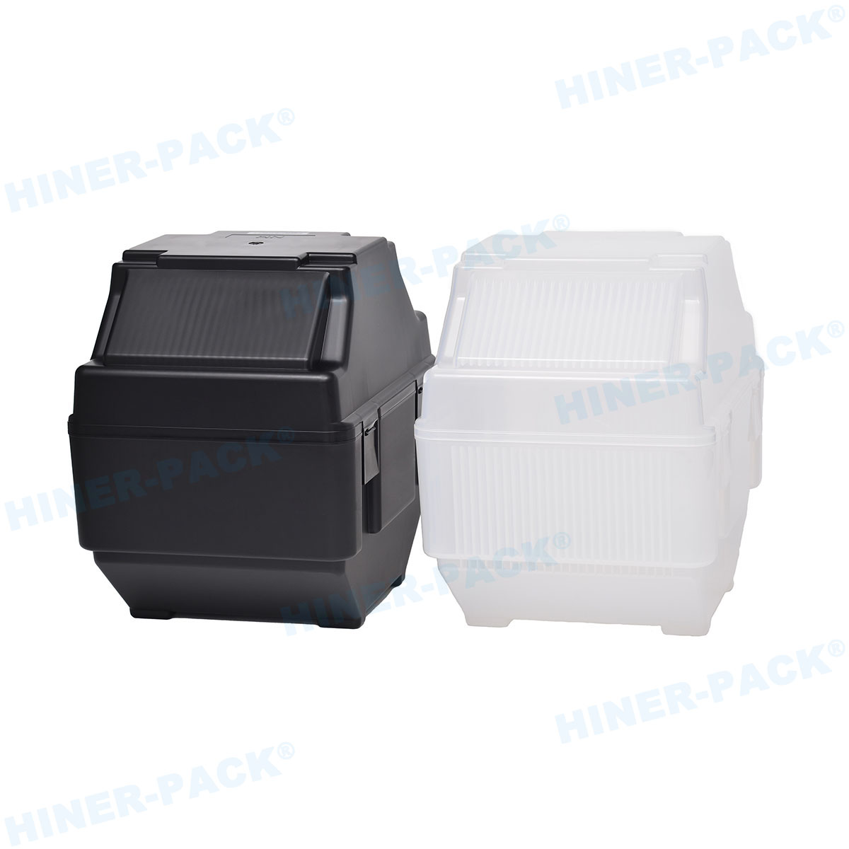
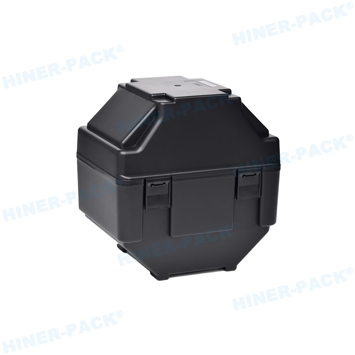
2. Structural Rib and Shell Design
The outer shell of a wafer cassette is not just a container. It is a structurally reinforced chassis. Through Finite Element Analysis (FEA), engineers design shells with strategic ribs and curves.
This design channels impact forces away from the wafer slots and into the strongest parts of the structure, much like a car's crumple zone.
3. Intelligent Latching and Sealing Mechanisms
A weak latch can fail upon impact, causing the container to open and eject the wafers. Advanced impact resistant wafer packaging features positive-action, robust latching systems. These latches are tested to remain securely closed even after multiple drops.
Combined with particle-free seals, they ensure both mechanical and environmental integrity.
Hiner-pack's Approach: Customized Protection for Every Node
At Hiner-pack, we understand that one size does not fit all. A 200mm power semiconductor wafer has different needs than a 300mm logic wafer. Our engineering philosophy is built on custom impact resistant wafer packaging solutions.
Our process involves:
Risk Assessment: Analyzing your supply chain for potential hazards.
Material Selection: Choosing the optimal combination of cushioning and structural polymers.
Prototype and Testing: Creating functional prototypes and subjecting them to ISTA and ASTM standard tests.
Validation and Mass Production: Ensuring every unit that leaves our facility meets the certified protection standard.
Application & Selection Guide: Choosing the Right Shipper
Selecting the correct packaging is a strategic decision. Here’s a quick guide:
For 300mm Advanced Logic Wafers (5nm and below): Prioritize maximum impact resistance with certified performance for drops over 1 meter. Look for ultra-low contamination materials and full automation compatibility. Hiner-pack's 300mm Nexus Series is designed for this exacting application.
For 200mm & MEMS Wafers: A balance of protection and cost-effectiveness is key. Robust, reusable shippers with good static control are ideal. Our 200mm Guardian Line offers superior protection for fab-to-fab transfers.
For Fragile Compound Semiconductor Wafers (e.g., GaAs, GaN): These wafers are often thinner and more brittle. Custom impact resistant wafer packaging with softer, conformal cushioning is essential to prevent edge chipping.
Key Selection Criteria:
Certified Drop Test Performance: Don't just take a vendor's word for it. Ask for the test data.
Material Purity: Ensure compliance with SEMI standards.
Automation Compatibility: Does it work with your SMIF and AMHS systems?
Total Cost of Ownership (TCO): Consider durability and reusability, not just the initial price.
The ROI of Investing in High-Performance Packaging
Viewing impact resistant wafer packaging as a cost center is a mistake. It is an insurance policy. The return on investment is clear:
Reduced Yield Loss: Eliminating breakage directly improves your bottom line.
Enhanced Supply Chain Reliability: No more costly delays due to damaged shipments.
Protection of R&D Investment: Safeguarding prototype and low-volume, high-value wafers is priceless.
Partnering with a specialist like Hiner-pack ensures you get a solution that delivers this ROI, not just a commodity container.
Future Trends: Smarter, More Integrated Packaging
The future of impact resistant wafer packaging is intelligent. We are developing solutions integrated with:
IoT Sensors: To monitor shock, temperature, and humidity in real-time.
RFID Tracking: For seamless inventory and chain-of-custody management.
Sustainable Materials: Creating high-performance, recyclable packaging without compromising protection.
Staying ahead of these trends is part of our commitment to providing the semiconductor industry with the protective solutions it needs to innovate fearlessly.
Frequently Asked Questions (FAQ)
Q1: What international standards should genuine impact resistant wafer packaging comply with?
A1: Reputable impact resistant wafer packaging should be tested and certified to recognized international standards. The most common are ISTA (International Safe Transit Association) procedures, particularly ISTA 3A for parcel delivery, and ASTM D5276 for drop testing. Compliance with SEMI standards for material purity and dimensional specifications is also critical for fab integration.
Q2: How many times can a typical Hiner-pack impact resistant wafer shipper be reused?
A2: The lifespan varies by model and application, but Hiner-pack shippers are engineered for robust reusability. Under normal handling conditions, our standard shippers are rated for 50+ cycles, while our premium models can exceed 100 cycles. Regular inspection of latches and seals is recommended to maintain performance.
Q3: Can you create custom packaging for non-standard wafer sizes or shapes?
A3: Absolutely. Custom impact resistant wafer packaging is a core specialty at Hiner-pack. We regularly engineer solutions for non-standard sizes, irregular shapes like quarter wafers, and highly fragile substrates like glass or compound semiconductors. Our engineering team works directly with clients to develop a perfect fit.
Q4: Beyond physical shock, what other hazards does this packaging protect against?
A4: While impact resistance is the primary function, a high-quality shipper offers multi-faceted protection. This includes shielding from static discharge (ESD) through conductive or dissipative materials, controlling contamination with low-outgassing polymers, and often providing a barrier against moisture and gaseous pollutants.
Q5: What is the typical lead time for a custom packaging solution from Hiner-pack?
A5: The lead time depends on the project's complexity. A standard custom impact resistant wafer packaging project, from design to first article delivery, typically takes 8-12 weeks. This includes prototyping, in-house testing, and client validation. We prioritize projects to align with our customers' critical timelines.


