
In the precision-driven world of semiconductor manufacturing, the margin for error is zero. A nanoscale particle, a minute electrostatic discharge, or a barely perceptible physical shock can compromise a wafer worth millions. While much attention is given to the fab process, the silent guardians of yield are often the secure wafer storage boxes that house these delicate substrates.
Choosing the right box isn't just about containment; it's about active protection. This guide breaks down the seven non-negotiable features that define best-in-class secure wafer storage boxes in 2024, ensuring your wafers are safeguarded from the cleanroom to the cargo hold.
Why "Secure" Goes Beyond a Simple Latch
A common misconception is that any wafer box provides adequate security. In reality, true security is a multi-layered concept. It encompasses:
Physical Integrity: Protection against impact, compression, and dust.
Electrostatic Shielding: Prevention of ESD-related damage.
Chemical Inertness: Ensuring no outgassing contaminates the wafer surface.
Mechanical Reliability: Consistent, particle-free operation over hundreds of cycles.
Standard boxes might check one or two of these boxes. High-performance secure wafer storage boxes are engineered to excel in all.
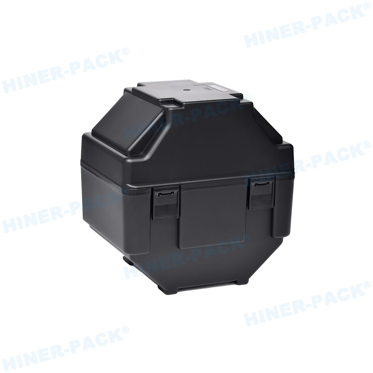
Feature 1: Advanced Mechanical Latching Systems
The latch is the gatekeeper. A flimsy latch can pop open upon impact, leading to catastrophic failure.
Look for a positive-action, dual-state latching mechanism. It should provide an audible or tactile click to confirm secure closure. The mechanism must be designed to withstand multiple drops without accidental release.
Hiner-pack's proprietary secure latching system is tested to MIL-STD standards for shock and vibration, offering unparalleled peace of mind.
Feature 2: Ultra-Low Particulate & Outgassing Materials
Contamination is a silent killer. The materials used in secure wafer storage boxes must be certified for cleanroom use.
This means using medical-grade or SEMI-standard polymers that are inherently low in particulates and have minimal outgassing of volatile organic compounds (VOCs). These compounds can condense on wafer surfaces, leading to defects.
Always request material certification data from your supplier.
Feature 3: Comprehensive ESD Protection
Electrostatic discharge can instantly destroy sensitive circuits. Protection cannot be an afterthought.
True secure wafer storage boxes are manufactured from static-dissipative or conductive materials. This creates a Faraday cage effect, shielding the wafers inside from external ESD events and preventing charge buildup within the box itself.
The surface resistance should be within a defined range (e.g., 10^5 to 10^11 ohms/sq) to safely control the dissipation of charge.
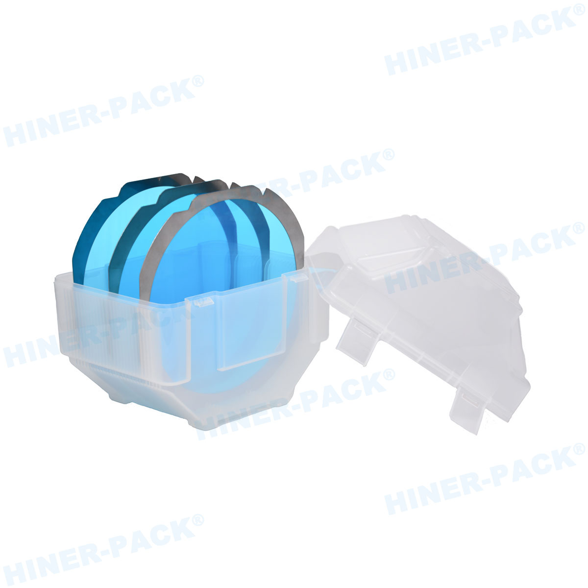
Feature 4: Precision-Molded Wafer Support
The internal supports that cradle each wafer are critical. Imperfections here can cause stress points, leading to micro-cracking, especially in ultra-thin wafers.
The supports must be precision-molded to exact tolerances, with smooth, radiused edges. The design should ensure minimal contact area while providing stable support, preventing wafer slippage and vibration during transport.
For custom secure wafer boxes, Hiner-pack utilizes 3D scanning to ensure a perfect fit for specific wafer profiles and thicknesses.
Feature 5: Robust Environmental Sealing
A secure box must be a sealed environment. An ineffective seal allows airborne molecular contaminants (AMCs), moisture, and particles to infiltrate the cavity.
A high-performance seal is made from perfluoroelastomer (FFKM) or similar inert materials. It must maintain integrity across a range of temperatures and pressures, such as those experienced during air freight.
This feature is paramount for long-term storage or inter-facility shipping.
Feature 6: Automation Compatibility (SMIF/FOUP Ready)
In modern fabs, manual handling is a bottleneck and a risk. Your secure wafer storage boxes must integrate seamlessly with automated material handling systems (AMHS), SMIF pods, and FOUP load ports.
This requires precise dimensional stability and robotic handling features. Inconsistent outer dimensions can cause misalignment and jams, leading to production downtime.
Hiner-pack designs its boxes with strict adherence to SEMI standards, guaranteeing compatibility with major automation platforms.
Feature 7: Traceability and RFID Integration
In Industry 4.0, the box itself can be a data carrier. Integrating RFID tags or 2D barcodes directly into the box structure enables seamless wafer tracking throughout the supply chain.
This allows for inventory management, chain-of-custody logging, and condition monitoring. It transforms a passive container into a smart asset.
We offer custom secure wafer storage solutions with embedded RFID for complete traceability.
The Hiner-pack Difference: Engineered Security
At Hiner-pack, we don't just manufacture boxes; we engineer wafer security systems. Our design philosophy is rooted in a deep understanding of semiconductor logistics and failure modes.
Every box in our product line is subjected to a rigorous validation protocol:
Drop Testing: ISTA 3A and ASTM D5276.
Compression Testing: Ensuring stackability in storage.
ESD Performance Testing: Verifying surface resistance and shielding effectiveness.
Outgassing Analysis: Using TGA-MS to identify and eliminate contaminant sources.
This commitment to validation is what sets our secure wafer storage boxes apart.
Application Guide: Matching the Box to the Need
Not all wafers have the same security requirements. Here’s a quick guide:
For 300mm Advanced Node Wafers (3nm/5nm): All seven features are mandatory. Prioritize the highest levels of contamination control and ESD protection. Our Nexus 300 series is built for this purpose.
For 200mm Power & MEMS Wafers: Focus on mechanical robustness, a reliable seal, and good ESD properties. The Guardian 200 line offers an optimal balance of performance and value.
For R&D and Prototype Wafers: Custom secure wafer boxes are often necessary. Hiner-pack can produce small batches with tailored internal configurations for non-standard substrates.
The True Cost of Insecurity: Why Investment Pays Off
Settling for inferior boxes is a false economy. The cost of a single failed wafer due to contamination or physical damage can outweigh the entire investment in a fleet of high-quality secure wafer storage boxes.
The Return on Investment is clear:
Higher Final Yield: Fewer in-line and end-of-line failures.
Reduced Downtime: No line stoppages due to damaged wafers from logistics.
Long-Term Asset Protection: Reusable, durable boxes protect your capital investment in silicon.
Don't let your weakest link be the box.
Frequently Asked Questions (FAQ)
Q1: What is the main difference between a standard wafer box and a "secure" wafer storage box?
A1: While a standard box provides basic containment, a secure wafer storage box is an engineered system designed for active, multi-faceted protection. The key differences lie in the certified mechanical latching, robust environmental sealing, superior ESD shielding, and the use of ultra-clean, low-outgassing materials that meet stringent SEMI standards.
Q2: Can Hiner-pack create custom secure wafer boxes for unusual wafer sizes, like 150mm or 100mm?
A2: Absolutely. We specialize in custom secure wafer storage solutions. We regularly engineer boxes for legacy wafer sizes (100mm, 125mm, 150mm) and non-standard shapes. Our process involves collaborative design and rapid prototyping to meet your exact specifications and substrate requirements.
Q3: How do I know if a wafer storage box provides adequate ESD protection?
A3: Reputable suppliers like Hiner-pack will provide certified test reports measuring surface and volume resistivity. Look for compliance with standards like ANSI/ESD S20.20. The box should be made of static-dissipative material (typically 10^6 to 10^9 ohms/sq) to safely control charge dissipation without being conductive enough to cause a rapid discharge.
Q4: Are your secure wafer boxes reusable, and what is their typical lifecycle?
A4: Yes, all Hiner-pack secure wafer storage boxes are designed for robust reusability. Under normal cleanroom handling conditions, our boxes are engineered for a lifecycle exceeding 500 open/close cycles. The longevity depends on the specific model and application, but we design for years of reliable service.
Q5: What is the lead time for a custom order of secure wafer boxes?
A5: Lead times vary based on the complexity of the customization. For a standard custom secure wafer box project, the typical lead time from design finalization to first article delivery is 8-10 weeks. This includes prototyping, tooling, and rigorous validation testing. We work closely with clients to meet critical project timelines.


