
In the intricate world of semiconductor manufacturing, precision and protection are paramount. Imagine a scenario where a tiny, fragile wafer—just 1 inch in diameter—holds the potential to power advanced electronics, yet it requires meticulous handling to avoid damage. This is where the 1 inch wafer carrier steps in, serving as an unsung hero in the production line. As industries push for miniaturization and higher yields, understanding this essential tool becomes crucial. Whether you're an engineer, a procurement specialist, or simply curious about semiconductor logistics, this article dives deep into the 1 inch wafer carrier, uncovering its significance from multiple angles. We'll explore its design, applications, and more, ensuring you grasp why this component is a cornerstone in modern technology. By the end, you'll have a comprehensive view of how the 1 inch wafer carrier safeguards innovation, one wafer at a time.
What Is a 1 Inch Wafer Carrier?
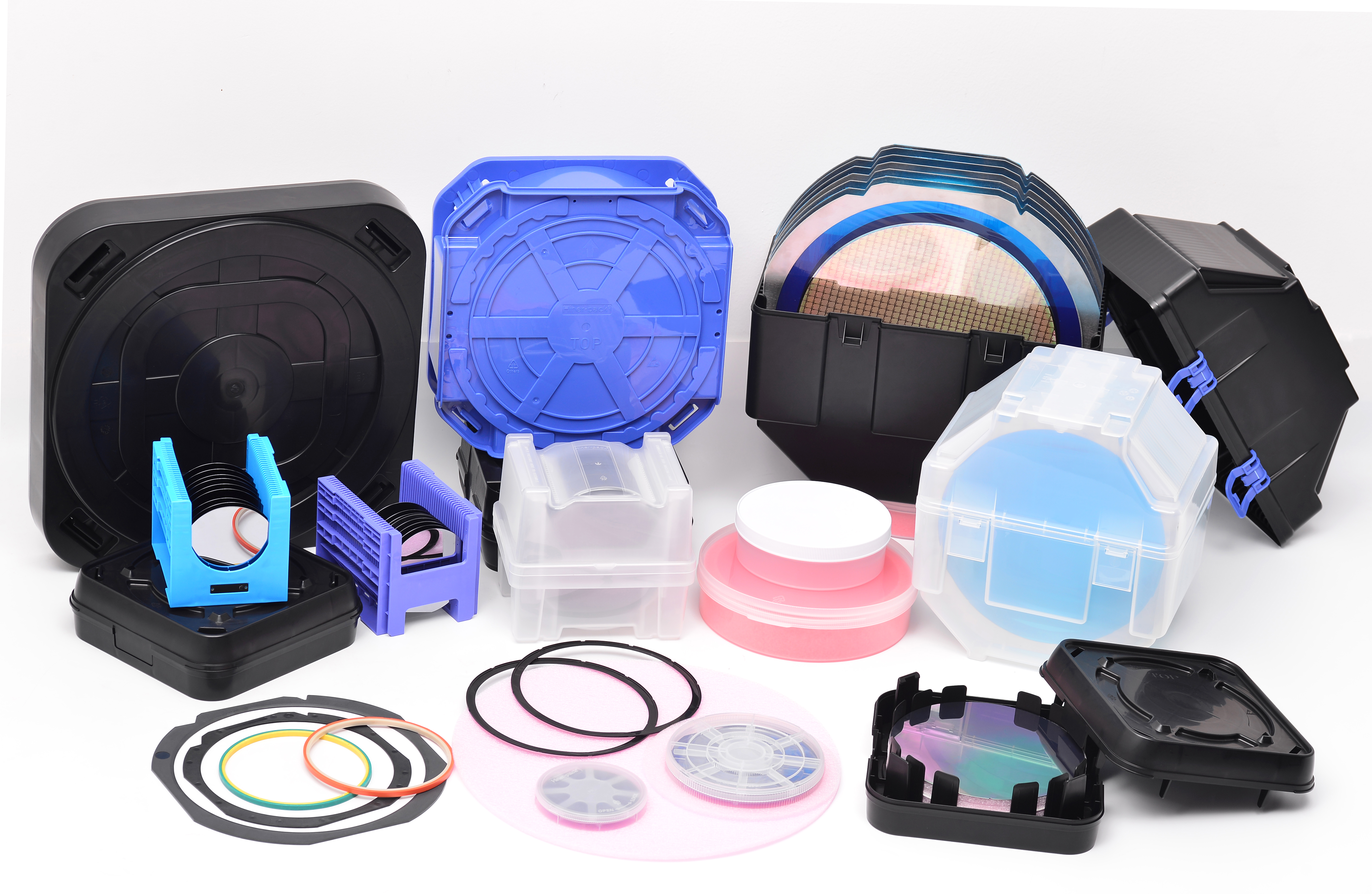
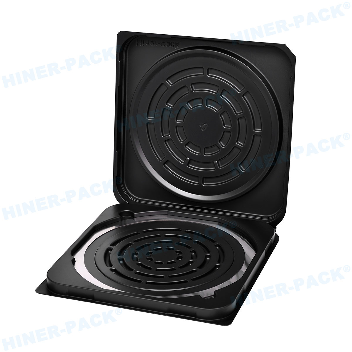
A 1 inch wafer carrier is a specialized container designed to hold, protect, and transport semiconductor wafers that measure approximately 1 inch in diameter. These wafers are thin slices of semiconductor material, such as silicon, used in the fabrication of microchips, sensors, and other electronic components. The 1 inch wafer carrier ensures that these delicate wafers remain uncontaminated and undamaged during storage, handling, and processing in cleanroom environments. Typically made from high-purity materials, the carrier features precise slots or grooves that cradle each wafer securely, preventing movement that could lead to scratches or breakage. This tool is integral to maintaining the integrity of wafers, which are often worth thousands of dollars due to their role in producing high-performance devices. In essence, the 1 inch wafer carrier acts as a protective shield, enabling efficient workflow in semiconductor facilities while minimizing waste and defects. Its compact size makes it ideal for research labs, pilot production lines, and applications involving small-scale wafers, where larger carriers would be impractical.
Key Design Features of 1 Inch Wafer Carrier
The design of a 1 inch wafer carrier is engineered for optimal performance and durability. First, materials selection is critical; carriers are often constructed from static-dissipative plastics, polycarbonate, or other composites that resist chemical corrosion and particulate generation. This ensures compatibility with harsh semiconductor processes, such as etching or deposition, without introducing contaminants. Second, the internal structure includes precisely molded slots that accommodate each 1 inch wafer individually, providing uniform support and reducing stress points. These slots are spaced to allow for easy loading and unloading, often with anti-tilt features to prevent wafers from shifting during transport. Additionally, many 1 inch wafer carriers incorporate RFID tags or barcodes for tracking purposes, enhancing traceability in automated systems. Ventilation holes are another common feature, facilitating proper airflow during cleaning or drying cycles. The exterior may include ergonomic handles and stacking capabilities, allowing for efficient storage in limited spaces. Overall, the design prioritizes cleanliness, mechanical stability, and user convenience, making the 1 inch wafer carrier a reliable component in high-stakes environments.
Applications in the Semiconductor Industry
The 1 inch wafer carrier finds extensive use across various segments of the semiconductor industry. In research and development, it enables scientists to experiment with novel materials and processes on small wafers, reducing costs and accelerating innovation. For instance, in universities and corporate labs, the 1 inch wafer carrier supports prototyping of new chip designs or MEMS (Micro-Electro-Mechanical Systems) devices. In production settings, it is employed in batch processing for specialized applications, such as optoelectronics or medical implants, where smaller wafers are standard. The carrier also plays a role in testing and quality control, allowing technicians to transport wafers between metrology tools without risk of damage. Moreover, in legacy system maintenance, the 1 inch wafer carrier ensures compatibility with older equipment that requires smaller wafer sizes. As the industry trends toward heterogeneous integration and IoT devices, the demand for precise handling of 1-inch wafers continues to grow, underscoring the carrier's versatility and importance in enabling cutting-edge technologies.
Advantages of Using 1 Inch Wafer Carrier
Utilizing a 1 inch wafer carrier offers several distinct advantages. Primarily, it enhances wafer protection by minimizing exposure to environmental hazards like dust, moisture, and physical impact. This leads to higher yield rates and reduced scrap, which is economically beneficial in high-volume manufacturing. The compact size of the 1 inch wafer carrier allows for efficient space utilization in cleanrooms and storage cabinets, enabling more wafers to be processed per square foot. Additionally, its lightweight design facilitates easier manual handling and reduces fatigue for operators, while compatibility with automation systems streamlines workflows. Another key benefit is cost-effectiveness; since 1-inch wafers are often used in low-volume or specialized production, the carrier helps lower overall expenses by preventing costly reworks. Furthermore, the reusability of high-quality 1 inch wafer carriers supports sustainability efforts, as they can be cleaned and reused multiple times without degradation. By investing in a reliable 1 inch wafer carrier, companies can achieve better process control and scalability, ultimately driving innovation in semiconductor applications.
Maintenance and Cleaning Procedures
Proper maintenance of a 1 inch wafer carrier is essential to ensure longevity and performance. Regular cleaning involves using deionized water, isopropyl alcohol, or specialized solvents to remove residues and particles without damaging the material. Automated cleaning systems, such as ultrasonic baths, are often employed to achieve high purity levels, followed by drying in controlled environments to prevent moisture buildup. Inspection should include checks for cracks, warping, or contamination, with damaged carriers replaced promptly to avoid wafer compromise. Storage recommendations for the 1 inch wafer carrier include keeping it in sealed containers or cleanroom-compatible bags when not in use, away from direct sunlight and extreme temperatures. Establishing a routine maintenance schedule—such as monthly cleanings for high-use scenarios—helps maintain the carrier's integrity. By adhering to these practices, users can extend the life of their 1 inch wafer carrier and uphold the strict cleanliness standards required in semiconductor operations.
Comparison with Other Wafer Carrier Sizes
When compared to larger carriers, such as those for 8-inch or 12-inch wafers, the 1 inch wafer carrier stands out for its niche applications. While larger carriers handle higher volumes and are common in mass production, the 1 inch wafer carrier excels in flexibility and precision for small-scale tasks. For example, it requires less storage space and lower material costs, making it ideal for prototyping or educational purposes. However, it may not offer the same economies of scale as bigger carriers in high-throughput fabs. In terms of design, the 1 inch wafer carrier often features simpler mechanics due to the smaller wafer size, but it must still meet rigorous cleanliness standards. This comparison highlights how the 1 inch wafer carrier complements broader industry needs by addressing specific requirements that larger formats cannot efficiently fulfill.
Future Trends in Wafer Carrier Technology
The evolution of the 1 inch wafer carrier is shaped by emerging trends in semiconductor technology. Advances in smart manufacturing are driving the integration of IoT sensors into carriers, enabling real-time monitoring of wafer conditions like temperature and humidity. Additionally, the push for sustainability is fostering the development of biodegradable or recyclable materials for the 1 inch wafer carrier, reducing environmental impact. As wafers become thinner and more fragile, future designs may incorporate enhanced cushioning and anti-vibration features. Automation and robotics will further optimize the handling of 1 inch wafer carriers, improving efficiency in miniaturized production lines. These innovations promise to make the 1 inch wafer carrier even more integral to next-generation semiconductor processes, supporting trends like AI-driven fabrication and quantum computing.
In summary, the 1 inch wafer carrier is a vital component in the semiconductor ecosystem, offering protection, efficiency, and versatility. From its precise design to its diverse applications, it enables advancements in technology while addressing the unique challenges of small-wafer handling. By understanding its facets, industry professionals can leverage the 1 inch wafer carrier to drive innovation and maintain competitive edges.
Frequently Asked Questions (FAQ)
Q1: What is the main function of a 1 inch wafer carrier?
A1: The main function of a 1 inch wafer carrier is to safely hold, store, and transport 1-inch semiconductor wafers during manufacturing processes, protecting them from contamination, physical damage, and environmental factors to ensure high yield and reliability.
Q2: How does a 1 inch wafer carrier differ from carriers for larger wafers?
A2: A 1 inch wafer carrier is specifically designed for smaller wafers, featuring compact dimensions and tailored slot spacing. Unlike larger carriers used in high-volume production, it prioritizes precision and flexibility for research, prototyping, and low-volume applications, often with simpler designs and lower material usage.
Q3: What materials are typically used in manufacturing a 1 inch wafer carrier?
A3: Common materials for a 1 inch wafer carrier include high-purity plastics like polycarbonate or PEEK, which offer chemical resistance, low particulate generation, and static dissipation. These materials are chosen to meet cleanroom standards and ensure compatibility with semiconductor processing environments.
Q4: Can a 1 inch wafer carrier be reused, and how should it be maintained?
A4: Yes, a 1 inch wafer carrier can be reused multiple times with proper maintenance. It should be regularly cleaned using deionized water or solvents, inspected for damage, and stored in clean, dry conditions. Following manufacturer guidelines helps extend its lifespan and maintain performance.
Q5: What are the key considerations when selecting a 1 inch wafer carrier?
A5: When selecting a 1 inch wafer carrier, consider factors such as material compatibility with your processes, slot design for wafer security, cleanliness certifications, durability, and compatibility with existing automation systems. Also, evaluate cost-effectiveness and support for tracking features like RFID to ensure it meets your operational needs.


