In the precision-driven field of semiconductor fabrication, the secure
transport of silicon substrates is a primary concern for yield management. The
silicon wafer, often carrying thousands of microscopic circuits, is vulnerable
to mechanical shock, electrostatic discharge, and molecular contamination.
Therefore, the selection of transport containers is not merely a procurement
task but a specialized engineering decision. Understanding the wafer shippers
price requires a deep dive into the material science and
manufacturing tolerances that these containers must satisfy to meet global
industry standards.
As microchip architectures shrink toward sub-5nm nodes, the tolerance for
environmental interference reaches near-zero levels. This necessitates advanced
packaging solutions that can maintain a controlled micro-environment during
international transit. Organizations like Hiner-pack have focused on
developing high-purity shipping solutions that address these complex
requirements while ensuring mechanical integrity throughout the supply
chain.
1. The Role of Material Science in Pricing Structures
The primary driver of the wafer shippers
price is the polymer composition used in the molding process. Not
all plastics are suitable for semiconductor environments. The industry demands
materials that exhibit low outgassing, high chemical resistance, and stable
electrostatic properties.
Polypropylene (PP) and Polycarbonate (PC) Applications
Standard transport boxes often utilize high-purity Polypropylene due to its
balance of flexibility and chemical inertness. However, for more demanding
applications where transparency and impact resistance are required,
Polycarbonate is the preferred choice. The procurement of medical-grade or
electronic-grade resins increases the raw material investment, which is
reflected in the final market valuation. These polymers must be free from heavy
metals and halogens to prevent any potential leaching onto the silicon
surface.
Carbon-Filled Resins for ESD Protection
Electrostatic Discharge (ESD) is a silent threat to semiconductor yield. To
mitigate this, manufacturers integrate conductive or dissipative carbon
additives into the polymer matrix. This specialized engineering ensures that the
surface resistivity remains within the requisite range of 10^4 to 10^9 ohms per
square. The precision required to achieve a uniform distribution of carbon
particles throughout the container walls significantly influences the wafer shippers
price, as any "hot spots" in resistivity can lead to catastrophic
component failure.
2. Engineering Design and Mechanical Dampening Systems
The structural architecture of a wafer shipper is designed to counteract the
physical stresses of global logistics. This includes vibration during air
transit and sudden G-force impacts during ground handling. A robust design must
prevent the wafer from shifting within its slot, which would otherwise lead to
edge chipping or surface scratching.
Horizontal vs. Coin-Style Architecture
Multi-Wafer Horizontal Shippers: Designed for high-volume
transport, these containers utilize internal combs or "teeth" to keep wafers
separated. The precision of these molds must be within microns to accommodate
various wafer thicknesses and prevent rattling.
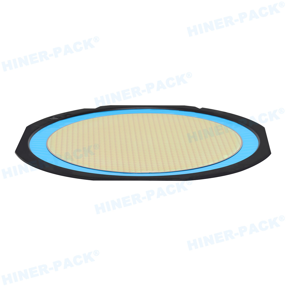
Single-Wafer Coin Shippers: Often used for high-value
compound semiconductors like Gallium Nitride (GaN) or Silicon Carbide (SiC),
these provide a secure, individualized environment. The complexity of the
screw-down or snap-fit lid mechanism plays a role in the wafer shippers
price.
Cushioning and Separation Material
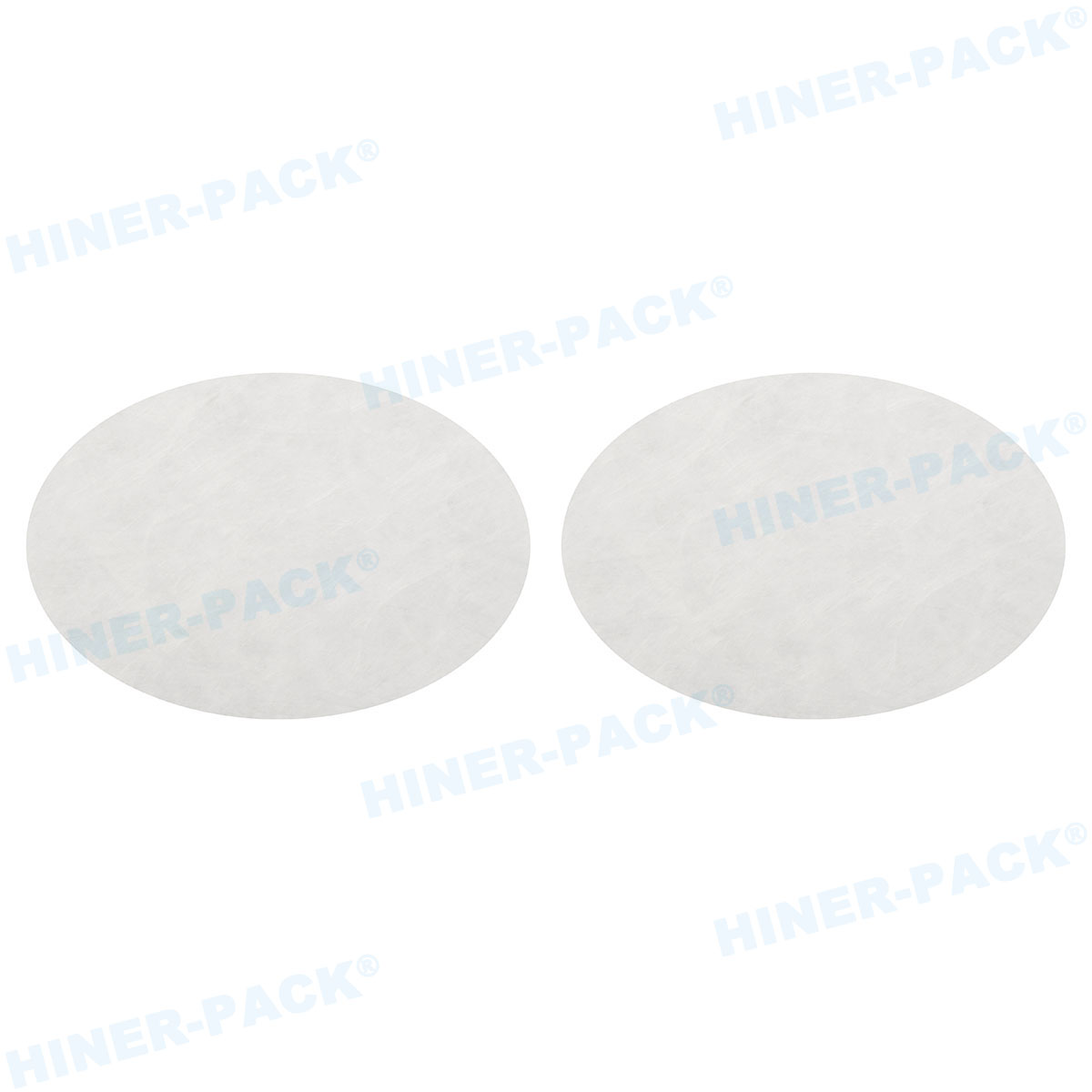
To further protect the delicate surface of the wafer, specialized interleaf
materials or cushions are often employed. These materials must be high-purity,
lint-free, and antistatic. The integration of these secondary components
requires rigorous testing to ensure they do not introduce particles or volatile
organic compounds (VOCs) into the sealed environment. Hiner-pack emphasizes the use of
specialized elastomer cushions that provide superior shock absorption without
compromising the cleanliness of the container.
3. Contamination Control and Cleanroom Manufacturing Standards
Semiconductor wafers are highly sensitive to Airborne Molecular Contamination
(AMC) and particulate matter. Therefore, the environment in which the shippers
are produced is a fundamental factor in the wafer shippers
price. A container that is molded and packaged in a standard
industrial facility is unsuitable for high-end semiconductor use.
ISO Class Cleanroom Requirements
Top-tier shippers are manufactured in ISO Class 5 or Class 6 cleanrooms. This
ensures that the containers are "clean-out-of-the-box," reducing the need for
extensive pre-washing by the end-user. The operational overhead of maintaining
these ultra-clean environments—including high-frequency HEPA filtration,
specialized garment protocols, and deionized water systems for
cleaning—contributes to the overall valuation of the product.
Outgassing and Haze Prevention
When wafers are stored for extended periods, the risk of "haze" formation due
to outgassing increases. Specialized low-outgassing materials are engineered to
minimize the release of molecules that could condense on the wafer surface.
Testing for these properties requires advanced gas chromatography and mass
spectrometry (GC-MS), adding a layer of quality assurance that differentiates
professional-grade shippers from low-cost alternatives.
4. Compatibility with Automated Fab Infrastructure
The transition toward Industry 4.0 and fully automated fabs has standardized
the physical requirements for wafer handling. Shipping boxes must be compatible
with Equipment Front End Modules (EFEM) and robotic vacuum wands. This
standardization is governed by SEMI (Semiconductor Equipment and Materials
International) guidelines.
SEMI Standard Compliance
Adherence to SEMI standards—such as M1 for wafer dimensions and various
standards for carrier geometry—ensures that the shipping containers can be
seamlessly integrated into automated sorting and inspection lines. The
investment in high-precision molds that meet these global specifications is a
significant factor. Containers that fail to meet these tolerances can cause
robotic handling errors, leading to line stoppages and potential hardware
damage.
By providing products that strictly follow these dimensions, Hiner-pack ensures that their
solutions are ready for immediate deployment in advanced manufacturing
facilities globally. The reliability of these dimensions is a pivotal component
of the wafer shippers
price, as it guarantees operational continuity.
5. Longevity and Multi-Cycle Usage
While the initial procurement focus is often on the immediate cost, the
durability of the shipper determines its long-term utility. High-quality
shippers are designed to be washed and reused across multiple shipping cycles.
This requires materials that can withstand the chemical stress of industrial
surfactants and the thermal stress of drying processes without losing their
structural or ESD properties.
Abrasion Resistance: The internal slots must resist wear
even after repeated loading and unloading of wafers.
Structural Rigidity: The container must not warp or deform
over time, as this would compromise the seal integrity and robotic
compatibility.
Environmental Stability: The ability to maintain protection
levels across varying temperatures and humidity levels during international
logistics is a hallmark of a high-performance shipping solution.
Prioritizing Quality in Semiconductor Logistics
The evaluation of wafer shippers
price must be approached through the lens of risk mitigation. In an
industry where a single contaminated lot can represent a loss of millions of
dollars, the shipping container is a necessary safeguard. From the selection of
carbon-loaded polymers to the precision of SEMI-compliant molding, every aspect
of these shippers is engineered to protect the most valuable assets in the
microelectronics supply chain.
As the sector continues to evolve with the rise of AI, 5G, and automotive
electronics, the demand for high-integrity transport solutions will only grow.
Selecting a partner that understands the nuance of contamination control and
mechanical protection is a crucial step for any semiconductor manufacturer or
assembly house.
Are you looking to optimize your wafer logistics with high-purity,
engineered shipping solutions? Contact our specialized team today to receive a
detailed quotation and technical consultation tailored to your specific
substrate requirements.
Frequently Asked Questions (FAQ)
Q1: What is the main factor that causes variations in wafer shippers
price between different suppliers?
A1: The most significant factors are the grade of the raw polymer, the
cleanroom classification used during manufacturing, and adherence to SEMI
standards. Higher-purity materials with documented low-outgassing properties and
ESD-stable additives naturally command a higher market value due to the
specialized manufacturing processes involved.
Q2: Can I use standard plastic boxes for transporting 300mm
wafers?
A2: No. 300mm wafers are extremely heavy and fragile. They require specific
Front Opening Shipping Boxes (FOSB) or specialized horizontal shippers that
manage the weight distribution and provide mechanical dampening. Using
non-specialized containers risks both physical breakage and chemical
contamination.
Q3: How does ESD protection in these shippers degrade over
time?
A3: In high-quality shippers where carbon is integrated into the polymer
matrix, the ESD properties are typically very stable. However, surface-treated
antistatic coatings can wear off or wash away. This is why "permanent" ESD
materials are preferred for multi-trip logistics despite the higher initial
investment.
Q4: Why is outgassing such a concern for wafer
transport?
A4: Outgassing occurs when volatile molecules are released from the plastic
container. In a sealed environment, these molecules can deposit onto the wafer,
creating a film that interferes with etching or bonding processes.
Low-outgassing materials are requisite for maintaining surface energy and
cleanliness.
Q5: Are there custom solutions available for non-standard wafer
thicknesses?
A5: Yes. While standard wafers follow SEMI specifications, specialized
applications like MEMS or thinned wafers for 3D packaging may require custom
internal supports or cushions to prevent vertical movement. Manufacturers like
Hiner-pack can often
provide customized inserts for these specific needs.
Q6: How should wafer shippers be cleaned before reuse?
A6: Shippers should be cleaned using automated ultrasonic systems with
deionized water and specialized surfactants. It is crucial to ensure that the
drying process does not introduce new particulates and that the temperature does
not exceed the polymer’s heat deflection point.


