In the high-precision environment of semiconductor manufacturing, the journey
of a processed wafer from the fabrication plant to the assembly and test
facility is fraught with potential hazards. Any compromise in the integrity of
the transport container can lead to catastrophic yield loss. As global demand
for high-performance microelectronics continues to surge, the industry requires
more than just simple storage boxes. Procuring the right wafer shippers
for sale involves a sophisticated understanding of polymer science,
mechanical vibration dampening, and stringent contamination control
protocols.
Modern integrated circuits, with their nanometer-scale features, are
susceptible to even the most minute environmental stresses. Whether dealing with
200mm or 300mm wafers, the packaging must serve as a mobile cleanroom. This
article examines the fundamental engineering requirements that define high-tier
transport solutions and how industry leaders like Hiner-pack address these complex
challenges through material innovation and structural design.
1. Material Science and ESD Mitigation in Wafer Transport
The choice of material for a wafer container is the first line of defense
against both physical and electrical damage. Standard polymers used in consumer
goods are insufficient for the semiconductor sector. Instead, manufacturers
utilize specialized blends of Polypropylene (PP), Polycarbonate (PC), or PEEK
(Polyetheretherketone) to ensure structural rigidity and chemical inertness.
Electrostatic Discharge (ESD) Protection
One of the primary concerns during transport is the buildup of static
electricity. Friction between the wafer and the container, or the container and
the external environment, can generate significant voltages. If this charge
discharges through the wafer, it can destroy the delicate circuitry.
High-performance wafer shippers
for sale are typically engineered with Carbon-Filled (CF) or
Carbon-Powdered resins to achieve specific surface resistivity ranges.
Antistatic: Provides a slow decay of static charges.
Static Dissipative: Allows charges to flow to ground in a
controlled manner, preventing sudden sparks.
Conductive: Offers the fastest grounding but must be used
carefully to avoid rapid discharge scenarios.
Outgassing and Chemical Purity
A second, often overlooked material property is outgassing. Many plastics
release volatile organic compounds (VOCs) over time. In a sealed wafer
container, these molecules can condense onto the wafer surface, causing "haze"
or interfering with subsequent lithography or deposition steps. Manufacturers
such as Hiner-pack prioritize low-outgassing materials that meet SEMI (Semiconductor Equipment and
Materials International) standards to maintain a pristine micro-environment for
the silicon substrate.
2. Structural Design for Mechanical Stability and Vibration Dampening
During air or ground transit, wafers are subjected to a wide spectrum of
vibration frequencies and sudden mechanical shocks. A wafer is essentially a
thin, brittle glass-like disc; even minor resonance can cause edge chipping or
micro-fractures. When evaluating wafer shippers
for sale, the internal architecture is just as vital as the
external shell.
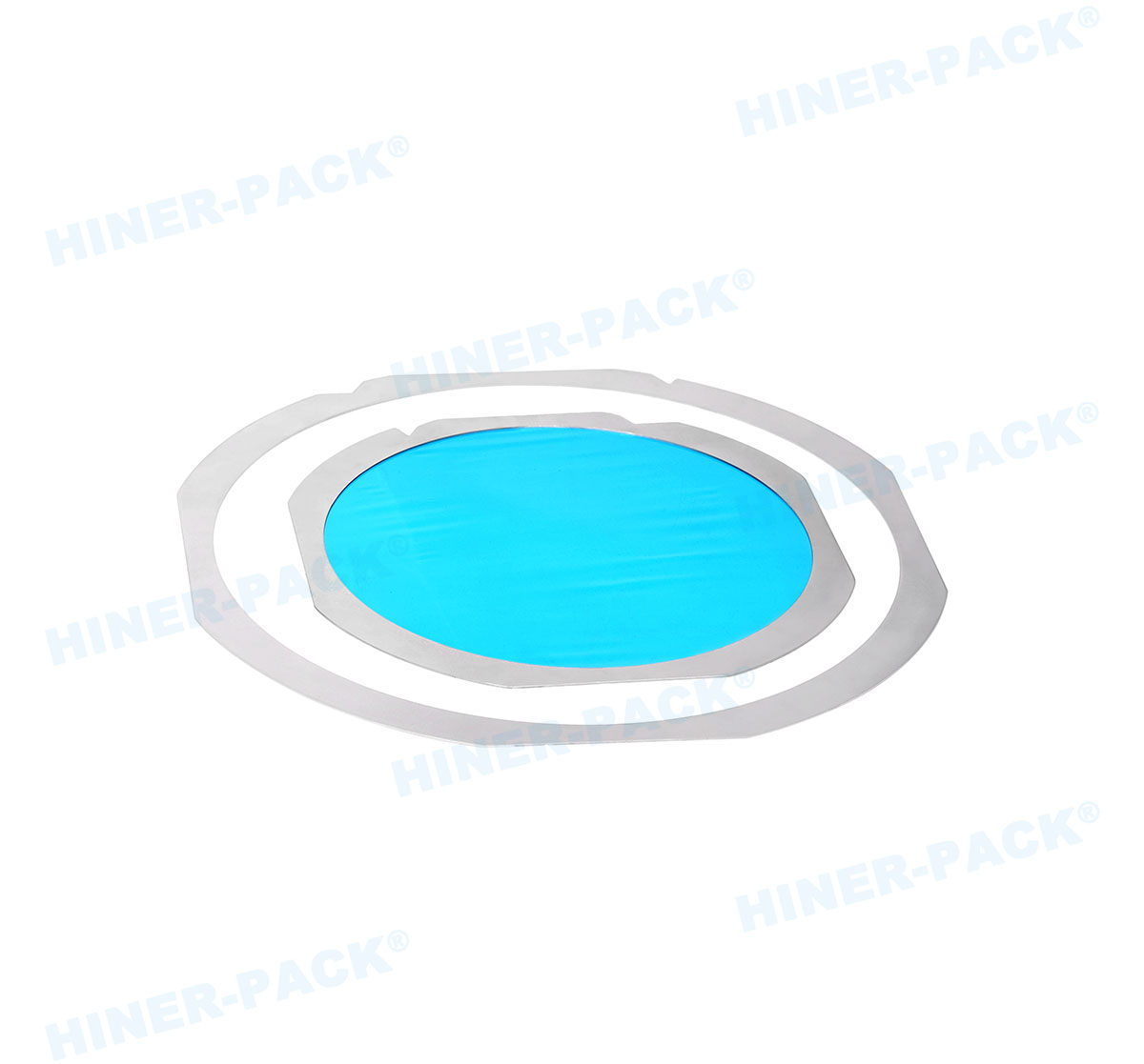
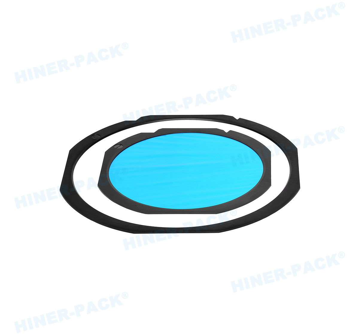
The Role of Cushions and Separators
Horizontal wafer shippers often incorporate internal cushioning systems.
These are not merely soft pads but are precision-engineered components designed
to absorb specific kinetic energy profiles. High-purity foams or specialized
elastomer springs are used to suspend the wafer stack, ensuring that the
G-forces experienced by the container do not reach the silicon itself. The
spacing between wafers must be maintained with absolute precision to prevent
"nesting" or surface-to-surface contact during turbulent transport
conditions.
Coin-Style vs. Multi-Wafer Carriers
The design philosophy differs based on the volume and type of wafer. For
single-wafer transport, often used for high-value R&D or compound
semiconductors (like GaN or SiC), "coin-style" shippers are preferred. These
feature a screw-top or snap-on lid that applies a controlled downward force,
securing the wafer against a flat, non-marring base. For volume production,
multi-wafer canisters or horizontal shippers allow for the efficient movement of
25-wafer lots while maintaining the same level of individual protection.
3. Contamination Management: The Silent Yield Killer
In the semiconductor world, a particle measuring 0.1 microns can be the
difference between a functional chip and a piece of scrap. The shipping
container must not only be clean when it leaves the factory but must actively
prevent the ingress of external particles and the generation of internal wear
debris.
Sealing Integrity
The interface between the lid and the base of the shipper must be perfectly
engineered. This often involves high-purity gaskets made of silicone or
fluoropolymers. A hermetic or near-hermetic seal prevents moisture vapor from
entering the container. High humidity can lead to the oxidation of metal layers
on the wafer, particularly in advanced nodes where copper or cobalt
interconnects are exposed. When sourcing wafer shippers
for sale, verifying the Moisture Vapor Transmission Rate (MVTR) is
a fundamental step for quality assurance teams.
Abrasion Resistance
Every time a wafer is loaded or unloaded, there is a risk of mechanical
abrasion between the wafer edge and the shipper's internal slots. This friction
can generate carbon particles or plastic micro-shards. Advanced shippers utilize
"low-sloughing" materials and polished contact surfaces to minimize particle
generation. This focus on "clean-by-design" is what separates professional-grade
logistics solutions from generic plastic containers.
4. Operational Compatibility with Automated Handling Systems
The modern fab is a sea of automation. Wafers are moved by Overhead Hoist
Transport (OHT) systems and loaded into tools by Equipment Front End Modules
(EFEM). Therefore, the physical dimensions of the shipping container must adhere
to rigid SEMI standards (such as M1 for wafer dimensions and dimensions for
carriers).
FOSB and FOUP Integration
For 300mm manufacturing, the Front Opening Shipping Box (FOSB) is the
standard. These containers are designed to be handled by robotic grippers and
feature precise kinematic coupling pins on the bottom to ensure they are seated
correctly on the load port. While Hiner-pack provides various
types of carriers, the industry trend is moving toward increasing the
intelligence of these containers, integrating RFID tags for real-time tracking
of wafer lots through the global supply chain. This connectivity reduces manual
handling errors and provides a complete chain of custody for every wafer
produced.
5. Environmental Considerations and Longevity
While the focus is often on the immediate protection of the wafer, the
sustainability and longevity of the shipping solution are increasingly relevant
in the B2B sector. High-quality shippers are designed for multiple reuse cycles.
This requires materials that can withstand rigorous cleaning processes,
involving deionized water and specialized surfactants, without degrading or
losing their ESD properties.
Rigorous testing protocols, including drop tests, stackability tests, and
thermal cycling, ensure that the wafer shippers
for sale can survive the harsh environments of international
shipping docks and pressurized aircraft cargo holds. A container that fails
after a single trip is not only a waste of resources but a risk to the fragile
cargo it carries.
6. Identifying High-Performance Solutions in a Crowded Market
When procurement managers look for wafer shippers
for sale, they must look beyond the price tag. The real value lies
in the reduction of risk. A single broken wafer in a 300mm lot can cost tens of
thousands of dollars in lost revenue, not to mention the potential for
downstream contamination in the fabrication tools.
Supplier Audits: Ensure the manufacturer operates within
ISO Class 5 or Class 6 cleanrooms for the final assembly and packaging of the
shippers.
Compliance Documentation: Request detailed reports on
surface resistivity, outgassing profiles, and particle counts.
Customization Capabilities: Sometimes, standard sizes do
not fit specific substrate thicknesses or fragile MEMS devices. Partnering with
a flexible manufacturer like Hiner-pack allows for tailored
solutions that meet unique engineering requirements.
Securing the Future of Semiconductor Yield
The logistics of semiconductor wafers is an exercise in microscopic risk
management. From the moment a wafer is diced or polished to the second it is
bonded in its final package, its safety depends on the container that holds it.
By focusing on material science, mechanical dampening, and strict contamination
control, manufacturers can ensure that their innovations reach their destination
in perfect condition.
As the industry pushes toward 2nm nodes and beyond, the requirements for
transport containers will only become more stringent. Selecting a partner who
understands the nuance of silicon transport is mandatory for maintaining a
competitive edge in the global market.
For organizations seeking reliable, high-purity transport containers, we
invite you to consult with our engineering team to discuss your specific
requirements. Protect your investment with industry-leading shipping
solutions.
For detailed specifications and bulk inquiries regarding our
specialized transport solutions, please contact our sales department today for a
formal quotation.
Frequently Asked Questions (FAQ)
Q1: What is the primary difference between a wafer carrier and a
wafer shipper?
A1: A wafer carrier is typically used for in-process handling within the
cleanroom and is often open-air or designed for chemical baths. A wafer shipper
is a secondary, sealed container designed to protect the wafers during external
transport, providing enhanced mechanical protection and environmental
sealing.
Q2: Why is ESD protection vital for unpatterned wafers?
A2: While unpatterned wafers (prime wafers) do not have circuits yet, static
charges can attract airborne molecular contamination and particulates to the
surface. These particles can cause "killer defects" during the first lithography
steps of the fabrication process.
Q3: How often can a high-quality wafer shipper be
reused?
A3: This depends on the cleaning protocol and the material. Polycarbonate and
PEEK shippers can often be reused dozens of times, provided they undergo
validated cleaning and inspection to ensure the ESD properties and structural
integrity remain intact.
Q4: Can these shippers be used for glass substrates or sapphire
wafers?
A4: Yes, while they are designed for silicon, they are compatible with any
substrate of the same diameter and thickness. For specialized materials like
sapphire or GaAs, custom internal cushions may be recommended due to different
brittle-fracture points.
Q5: What certifications should I look for when purchasing wafer
shipping containers?
A5: Look for SEMI standard compliance (specific to the size of your wafer),
RoHS and REACH compliance for material safety, and ISO 9001 certification for
the manufacturer’s quality management system.
Q6: How do you prevent wafers from rattling during air
transport?
A6: High-end shippers use a "top-pressure" design or specialized separators
that apply a gentle, constant force to the wafer stack, neutralizing the gap
between the wafer and the container wall, which prevents movement during
turbulence.


