In the heart of every smart device, car, and data center lies a semiconductor chip, a marvel of modern engineering. The journey of creating these chips is a symphony of precision, conducted within the ultra-clean environments of wafer fabs. At every step of this intricate process, from crystal growth to final packaging, the silicon wafer must be moved, stored, and positioned with near-absolute accuracy. This is the critical, though often overlooked, domain of wafer handling equipment. This equipment forms the backbone of the material handling automation within a fab, ensuring that multi-thousand-dollar wafers are transported without contamination, damage, or misalignment. The evolution of this technology, particularly the shift to larger wafer sizes, has been pivotal in driving down costs and boosting output. This article delves into five key areas where advanced wafer handling solutions are fundamentally transforming semiconductor manufacturing, ensuring the industry can keep pace with relentless technological demands.
The Critical Role of Wafer Handling in the Fab Ecosystem
Semiconductor fabrication is arguably the most complex manufacturing process ever devised. A single wafer can undergo hundreds of process steps, taking weeks to complete. Wafer Fab Equipment (WFE) represents the multi-billion-dollar collection of tools that perform these steps—lithography, etching, deposition, and inspection. However, these sophisticated tools are islands of automation without a reliable bridge between them. That bridge is the Wafer Handling System.
A single particle, a minute scratch, or a slight misalignment can render a wafer useless, wasting thousands of dollars and precious production time. Therefore, the primary mission of any wafer handling equipment is to move wafers between process tools, storage units, and measurement stations with zero damage and zero contamination. This requires systems built with materials that do not outgas, robots with exceptional precision (often with micron-level repeatability), and sophisticated software that orchestrates every movement. The integrity of the entire manufacturing line hinges on the reliability of its handling systems.
The 300mm Standard: Precision at Scale
The industry's dominant standard for over two decades, the 300mm wafer, offers more than double the surface area of its 200mm predecessor. This allows for the production of many more chips per wafer, significantly improving economies of scale. However, handling these larger, thinner, and more valuable substrates presents unique challenges. 300mm Wafer Handling is characterized by highly automated, standardized systems.
FOUPs and AMHS: The Front-Opening Unified Pod (FOUP) is the universal container for 300mm Wafer Handling. It holds up to 25 wafers in a sealed, nitrogen-purged environment, protecting them from particles and humidity during transport. An Automated Material Handling System (AMHS)—a network of overhead hoists, rail-guided vehicles, and stockers—manages the movement of these FOUPs throughout the fab. This "hands-off" approach is essential for maintaining yield in a 300mm environment.
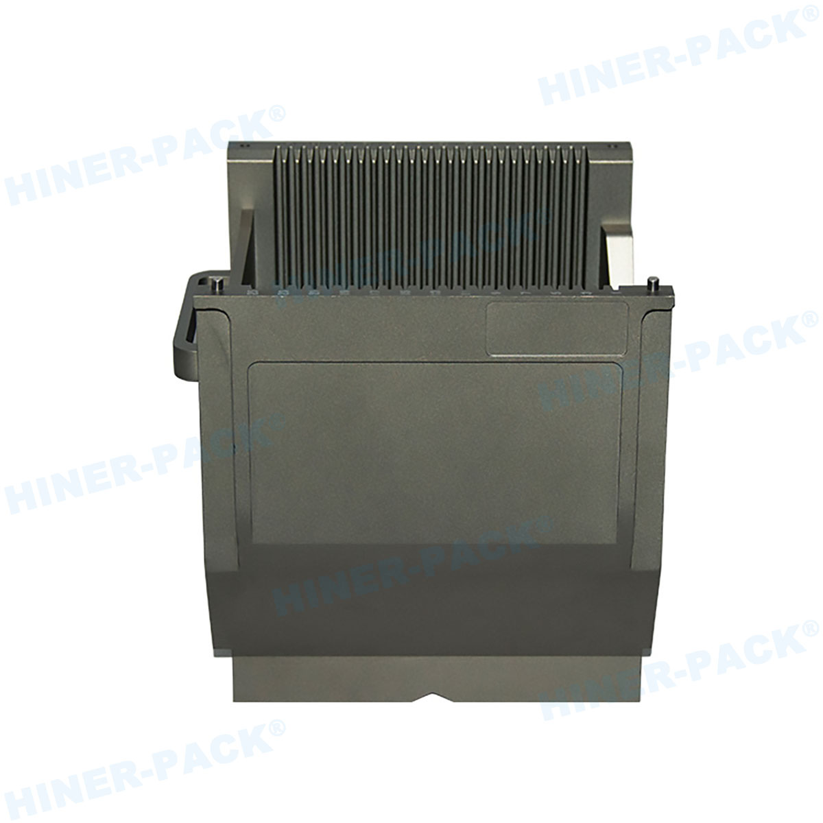
Advanced Robotics: Inside each piece of Wafer Fab Equipment, a sophisticated robotic arm is responsible for the delicate task of picking wafers from the FOUP and placing them onto the process chamber's chuck. These robots must be incredibly fast to maximize throughput, yet gentle and precise to avoid damaging the wafer's edges and patterned surfaces. The design of these internal handlers is a critical differentiator for equipment manufacturers.
The Resilient World of 200mm and Legacy Fabs
While cutting-edge logic fabs have moved to 300mm and are pioneering 450mm prototyping, a significant portion of the semiconductor industry still thrives on 200mm Wafer Handling. Many analog, power, and MEMS (Micro-Electro-Mechanical Systems) chips are ideally suited for 200mm fabs, which often have fully depreciated equipment, making them highly cost-effective for these specific markets.
The demands of 200mm Wafer Handling are different. While automation exists, it is less ubiquitous than in 300mm fabs. Many 200mm lines still use SMIF (Standard Mechanical Interface) pods or even open cassettes, requiring different types of handling robotics. Furthermore, there is a massive installed base of legacy Wafer Fab Equipment that requires maintenance, upgrades, and replacement parts for their integrated Wafer Handling System. Companies that provide reliable wafer handling solutions for these mature technologies play a vital role in the global semiconductor supply chain, ensuring the continued production of essential chips for automotive, industrial, and consumer applications.
Innovations in Wafer Handling Solutions for Next-Generation Challenges
As semiconductor technology advances, so too must the wafer handling equipment that supports it. Several key trends are driving innovation:
Thinner Wafers and Warpage Control: For 3D NAND flash memory and advanced packaging techniques like fan-out, wafers are thinned down to mere microns. These wafers are highly prone to warping, making them incredibly difficult to pick and place reliably. New end-effector designs with advanced sensing and gentle, multi-point contact are being developed to handle this challenge.
Contamination Control to the Atomic Level: With chip features now measured in nanometers, the tolerance for contamination has shrunk to atomic levels. Wafer handling solutions are evolving to use new, ultra-clean materials, coatings that minimize static charge, and enhanced purge systems to eliminate any possibility of molecular contamination.
AI and Predictive Maintenance: Unplanned downtime in a fab can cost millions of dollars per day. Modern Wafer Handling Systems are increasingly equipped with sensors and AI-driven software that monitor the health of robots in real-time. They can predict bearing wear, motor degradation, or alignment drift before they cause a failure, allowing for maintenance to be scheduled during planned tool downtime.

The Hiner-pack Approach to a Robust Wafer Handling System
In this demanding landscape, manufacturers rely on partners who understand the nuances of semiconductor manufacturing. A company like Hiner-pack, with its focus on the international semiconductor sector, exemplifies the expertise required. Hiner-pack doesn't just supply components; it provides integrated wafer handling solutions designed for maximum uptime and yield.
Whether it's for a brownfield 200mm Wafer Handling upgrade or a new 300mm tool, Hiner-pack engineers its systems with a focus on reliability, precision, and cleanroom compatibility. By understanding the entire ecosystem of Wafer Fab Equipment, they can deliver a Wafer Handling System that seamlessly integrates with a customer's specific process flow, ensuring that the vital task of wafer transport is a source of strength, not a point of failure.
From the robust demands of legacy 200mm fabs to the high-throughput, fully automated world of 300mm production, wafer handling equipment is the unsung hero of the semiconductor industry. It is the critical enabler that allows Moore's Law to persist, ensuring that wafers can navigate the increasingly complex fab landscape safely and efficiently. The continuous innovation in wafer handling solutions—smarter, cleaner, and more precise—will remain foundational to producing the powerful chips that will drive future technologies, from AI to quantum computing. As the industry pushes forward, the reliability of every Wafer Handling System will continue to be a direct determinant of manufacturing success.
Frequently Asked Questions (FAQs)
Q1: What is the primary difference between a 200mm and a 300mm Wafer Handling System?
A1: The most significant difference is the level of automation and the container used. 300mm Wafer Handling relies almost exclusively on fully automated systems using FOUPs (Front-Opening Unified Pods) and an overhead transport system. 200mm Wafer Handling, while often automated, more frequently uses SMIF pods or open cassettes and may involve more manual or semi-automated transport methods, especially in older fabs.
Q2: Why is contamination control so critical in wafer handling equipment?
A2: Semiconductor features are now smaller than the wavelength of visible light. A microscopic particle that is invisible to the human eye can be as large as a "boulder" on a chip's circuitry, completely destroying several dies. Wafer handling equipment is designed with special materials, coatings, and cleanroom-compliant mechanisms to prevent the generation and transfer of any particles, ensuring the pristine condition of the wafer.
Q3: Can older 200mm Wafer Fab Equipment be upgraded with modern handling solutions?
A3: Yes, absolutely. This is a key service provided by specialized companies like Hiner-pack. Upgrading the internal Wafer Handling System of a legacy tool can dramatically improve its reliability, throughput, and yield. This can involve replacing old robots with newer, faster, and more precise models, or updating the software and sensors to enable better diagnostics and predictive maintenance.
Q4: What role does software play in a modern Wafer Handling System?
A4: Software is the "brain" of the system. It controls the complex trajectories of the robotic arms, manages the communication between the tool and the fab's host computer, and orchestrates the sequence of wafer movements. Advanced software also enables real-time monitoring, collecting data on robot performance to predict maintenance needs and prevent unplanned downtime, which is crucial for fab productivity.
Q5: How are wafer handling solutions adapting to the challenges of advanced packaging?
A5: Advanced packaging, such as 2.5D and 3D integration, often involves handling thinned wafers that are highly flexible and prone to warping. Wafer handling solutions are adapting with new end-effector technologies that distribute vacuum or use electrostatic forces more evenly to pick up bowed wafers without causing stress or breakage. Furthermore, handling systems are being designed to manage temporary bonding and debonding carriers that support these ultra-thin wafers through the process flow.


