In the highly precise world of semiconductor manufacturing, every component plays a vital role. Among the most crucial, yet sometimes overlooked, is the semiconductor wafer carrier. This piece of equipment is not merely a container; it is the primary guardian of the delicate silicon wafers upon which billions of transistors are built. From the foundry to the fabrication line, the integrity of these wafers is paramount, and the carrier ensures they remain free from contaminants, physical damage, and electrostatic discharge. This article delves into seven essential aspects of semiconductor wafer carriers, providing a comprehensive look at their technology, selection criteria, and the economics behind their manufacturing.
1. More Than a Box: The Fundamental Role of a Wafer Carrier
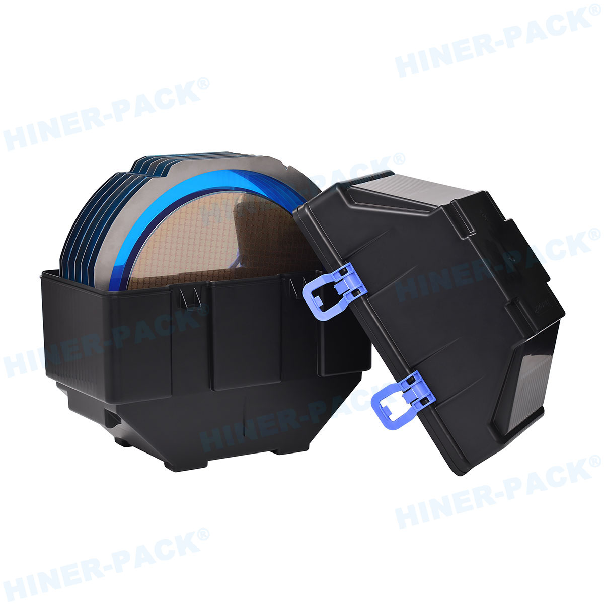
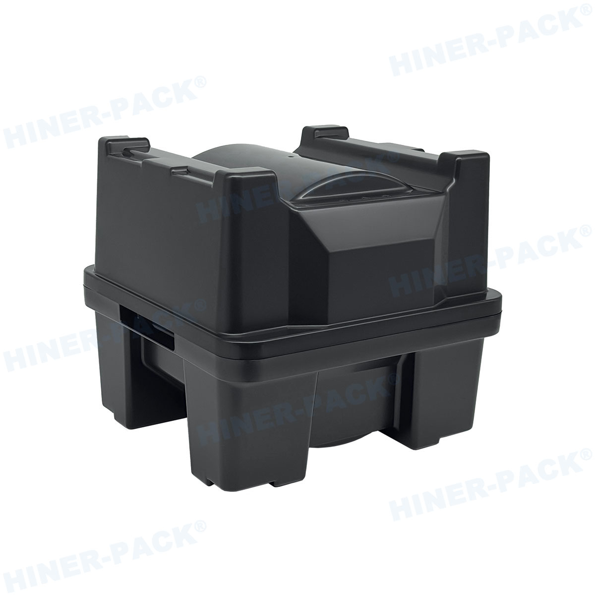
A semiconductor wafer carrier, also commonly referred to as a FOUP (Front-Opening Unified Pod) for 300mm wafers or a FOSB (Front-Opening Shipping Box) for transportation, is a precision-engineered container. Its primary function is to safely house, transport, and store silicon wafers in a controlled mini-environment throughout the manufacturing process. As wafers move through hundreds of process steps, the carrier protects them from airborne particles, moisture, and physical shock. The choice of an appropriate carrier directly impacts yield rates—a single particle-induced defect can render a multi-thousand-dollar wafer useless. Therefore, partnering with a reliable wafer carrier manufacturer is a strategic decision for any semiconductor fab.
2. A Deep Dive into Materials and Manufacturing technology
The construction of a wafer carrier is a lesson in advanced materials science. For decades, polycarbonate has been a popular choice due to its toughness and clarity. However, as process nodes have shrunk to 5nm and below, the industry has shifted toward more advanced materials.
PEEK (Polyetheretherketone): Known for its excellent chemical resistance, low outgassing, and ability to withstand high temperatures encountered in processes like ion implantation.
PFA (Perfluoroalkoxy alkane): Offers superior purity and is often used in wet process stations due to its exceptional resistance to harsh chemicals.
Advanced Composites: New carbon-fiber and particle-filled composites are being developed to achieve the ultimate balance of static dissipation, dimensional stability, and lightweight properties.
The manufacturing process itself is a precision endeavor. It involves injection molding with tightly controlled parameters to prevent stress and warpage, followed by rigorous machining to meet exacting tolerances. The internal ribs that cradle the wafers must be perfectly contoured to minimize contact points and prevent wafer sliding or chipping.
3. Navigating the Selection Process: A Practical Guide
Choosing the right semiconductor wafer carrier is not a one-size-fits-all decision. Several factors must be considered to ensure compatibility and performance within a specific fab environment.
Wafer Size and Capacity: The most obvious differentiator. While 200mm and 300mm are standard, the industry is gradually adopting 450mm for future nodes, requiring entirely new carrier designs.
Material Compatibility: The carrier material must be inert to the chemicals and plasmas it will be exposed to. A custom wafer carrier might be necessary for unique process chemistries.
Automation Compatibility: The carrier must interface flawlessly with the fab's automated material handling systems (AMHS). This includes precise dimensions for robotic handling and standardized latching mechanisms.
Static Control: With increasingly sensitive circuits, controlling electrostatic discharge (ESD) is critical. Carriers are often classified as Static Dissipative or Conductive to safely ground any potential charge.
4. The Price Equation: Understanding Wafer Carrier Costs
The price of a wafer carrier can vary dramatically, from a few hundred to several thousand dollars per unit. This wide range is influenced by several key factors:
Material Cost: High-performance polymers like PEEK are significantly more expensive than standard polycarbonate.
Complexity and Precision: A carrier designed for 25 wafers with intricate RFID and environmental monitoring features will cost far more than a basic 13-wafer storage box.
Volume and Customization: A large order of standard carriers will have a lower per-unit cost than a small batch of highly customized carriers. The engineering and tooling costs for custom designs are substantial.
Certification and Testing: Carriers that come with full traceability, lot-specific data, and certification for specific cleanroom classes command a higher price.
When evaluating cost, it's essential to consider the Total Cost of Ownership (TCO), which includes not just the initial purchase price but also the carrier's lifespan, maintenance requirements, and its impact on overall yield.
5. The Rise of the Custom Wafer Carrier
As semiconductor processes become more specialized, the demand for custom wafer carriers is growing. A standard off-the-shelf solution may not suffice for applications involving extreme temperatures, unique wafer geometries (like thin wafers for power devices), or integrated sensors for real-time environmental monitoring. A proficient wafer carrier manufacturer will work closely with clients to design a carrier that meets specific mechanical, chemical, and electrical requirements. This collaborative process, while involving a higher initial investment, can lead to significant long-term gains in process efficiency and product yield.
6. Finding the Right Partner: A Supplier Checklist
Selecting a wafer carrier manufacturer or supplier is as critical as selecting the carrier itself. A reliable partner ensures consistent quality, supply chain stability, and technical support. Key criteria for selection include:
Proven Expertise and Experience: Look for a manufacturer with a long track record in the semiconductor industry.
Quality Certifications: Compliance with international standards like ISO 9001 and IATF 16949 is a baseline.
R&D Capability: A supplier that invests in research and development is better positioned to solve future challenges.
Global Support and Logistics: The ability to supply and support your operations worldwide is crucial for multinational fabs.
7. The Future: Smart Carriers and Industry 4.0
The next frontier for the semiconductor wafer carrier is intelligence. The concept of the "smart FOUP" is gaining traction. These carriers are equipped with embedded sensors that can monitor internal conditions such as humidity, oxygen levels, vibration, and even wafer identity in real-time. This data, integrated into a fab's Industry 4.0 framework, allows for predictive maintenance, better lot tracking, and immediate corrective actions if the wafer's environment is compromised. This evolution transforms the carrier from a passive container to an active, data-generating component of the manufacturing process.
Frequently Asked Questions (FAQs)
Q1: What is the typical lifespan of a semiconductor wafer carrier?
A1: The lifespan of a semiconductor wafer carrier varies significantly based on the material, the processes it's exposed to, and handling practices. In a high-volume fab, a polycarbonate FOUP might last 2-5 years before showing signs of wear like cracking or increased particle generation. Carriers made from more robust materials like PEEK can last considerably longer. Regular cleaning and preventive maintenance are essential to maximize their service life.
Q2: How often do wafer carriers need to be cleaned, and what methods are used?
A2: The cleaning frequency depends on the fab's protocols and the specific process tools the carrier visits. It can range from every few cycles to a fixed schedule (e.g., weekly). Cleaning methods include deionized water rinses, chemical baths with solvents, and advanced techniques like cryogenic aerosol or plasma cleaning to remove stubborn molecular contaminants without damaging the carrier material.
Q3: What are the key differences between a FOUP and a FOSB?
A3: A FOUP (Front-Opening Unified Pod) is designed for use within the semiconductor fabrication cleanroom. It interfaces directly with process tools and the Automated Material Handling System (AMHS). A FOSB (Front-Opening Shipping Box) is primarily used for the shipping and long-term storage of wafers between different facilities. FOSBs are generally more robust to withstand the rigors of transportation but are not typically used on the fab line itself.
Q4: Can a damaged wafer carrier be repaired, or must it be replaced?
A4: Minor damage, such as a broken latch or a worn-out seal, can often be repaired by replacing the individual component. However, if the main body of the carrier is cracked, warped, or has damaged wafer slots that could pose a risk to the wafers, replacement is the only safe option. Continuing to use a compromised carrier poses a significant contamination and yield risk.
Q5: How does the price of a custom wafer carrier compare to a standard one?
A5: The price of a custom wafer carrier is substantially higher than a standard model. This is due to the non-recurring engineering (NRE) costs associated with the design, prototyping, and testing phases, as well as the cost of creating custom injection molds. For a standard carrier, these development costs are amortized over millions of units, whereas for a custom solution, they are borne by a much smaller production run, leading to a higher per-unit price.


