In the fast-paced world of semiconductor manufacturing, efficiency and precision are paramount. At the heart of this industry lie semiconductor wafer handling tools, which ensure that delicate wafers are moved, stored, and processed without damage. As technology advances, the demand for more sophisticated handling solutions has grown, particularly with the shift toward larger wafer sizes like 300mm and the exploration of 450mm standards. This article delves into the key tools and systems driving this evolution, including Automated Material Handling System (AMHS) solutions, Equipment Front End Module (EFEM) integrations, and Advanced Wafer Handling Solutions from industry leaders like Hiner-pack. We'll explore how these innovations are addressing challenges in contamination control, throughput, and scalability, while maintaining a focus on practical applications in today's fabs. By understanding these components, manufacturers can optimize their operations and stay competitive in a global market. Let's dive into the details, starting with the foundational aspects of wafer handling and progressing to cutting-edge advancements.
The Evolution of Wafer Sizes: From 300mm to 450mm
The semiconductor industry has undergone significant transformations in wafer sizes, primarily driven by the need for higher productivity and cost-efficiency. 300mm wafer handling tools have become the standard in most modern fabrication facilities, enabling the production of more chips per wafer and reducing overall costs. These tools are designed to handle wafers with diameters of 300mm (approximately 12 inches), requiring precise robotics and contamination-free environments to prevent defects. For instance, 300mm wafer handling tools often incorporate advanced sensors and grippers to minimize particle generation during transfer, which is critical for maintaining yield rates in high-volume manufacturing.
However, as the industry looks toward the future, 450mm wafer handling has emerged as a potential next step. Although not yet widely adopted due to high infrastructure costs and technical hurdles, 450mm wafer handling promises even greater economies of scale by allowing up to twice the number of chips per wafer compared to 300mm. This transition demands robust semiconductor wafer handling tools capable of managing the increased weight and fragility of larger wafers. Challenges include developing stronger materials for handlers and optimizing transport systems to avoid stress-induced cracks. Companies like Hiner-pack are at the forefront, researching 450mm wafer handling solutions that integrate seamlessly with existing Automated Material Handling System frameworks. By addressing these issues, the industry aims to reduce per-chip costs and support the growing demand for semiconductors in applications like AI and IoT.
Automated Material Handling Systems: Boosting Efficiency in Fabs
An Automated Material Handling System (AMHS) is a cornerstone of modern semiconductor manufacturing, automating the movement of wafers between process tools, storage areas, and metrology stations. This system reduces human intervention, minimizing contamination risks and improving throughput. In practice, an Automated Material Handling System typically includes overhead hoists, conveyors, and robotic vehicles that transport wafer carriers, such as Front Opening Unified Pods (FOUPs). For example, in a fab using 300mm wafer handling tools, the AMHS ensures that wafers are delivered on time to etching or deposition equipment, synchronized via software controls.
The integration of semiconductor wafer handling tools with AMHS enhances overall operational efficiency. By leveraging real-time data analytics, these systems can predict maintenance needs and optimize routing, reducing downtime. Hiner-pack, as an international leader in this field, offers tailored Automated Material Handling System solutions that support both 300mm wafer handling tools and future-ready 450mm wafer handling setups. Their systems emphasize scalability, allowing fabs to expand without major overhauls. Moreover, the role of an Automated Material Handling System extends beyond transport—it includes environmental controls to maintain cleanroom standards, which is vital for yield preservation. As fabs adopt more interconnected processes, the AMHS becomes a critical enabler of Industry 4.0, driving smarter, more responsive manufacturing environments.
Equipment Front End Modules: Streamlining Wafer Processing
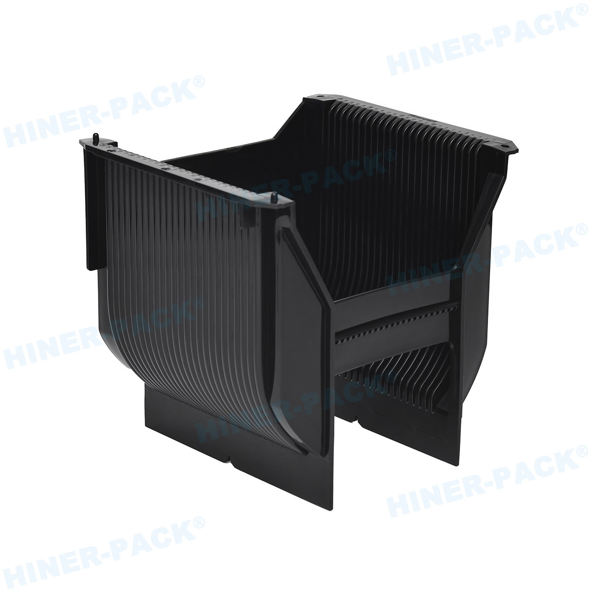
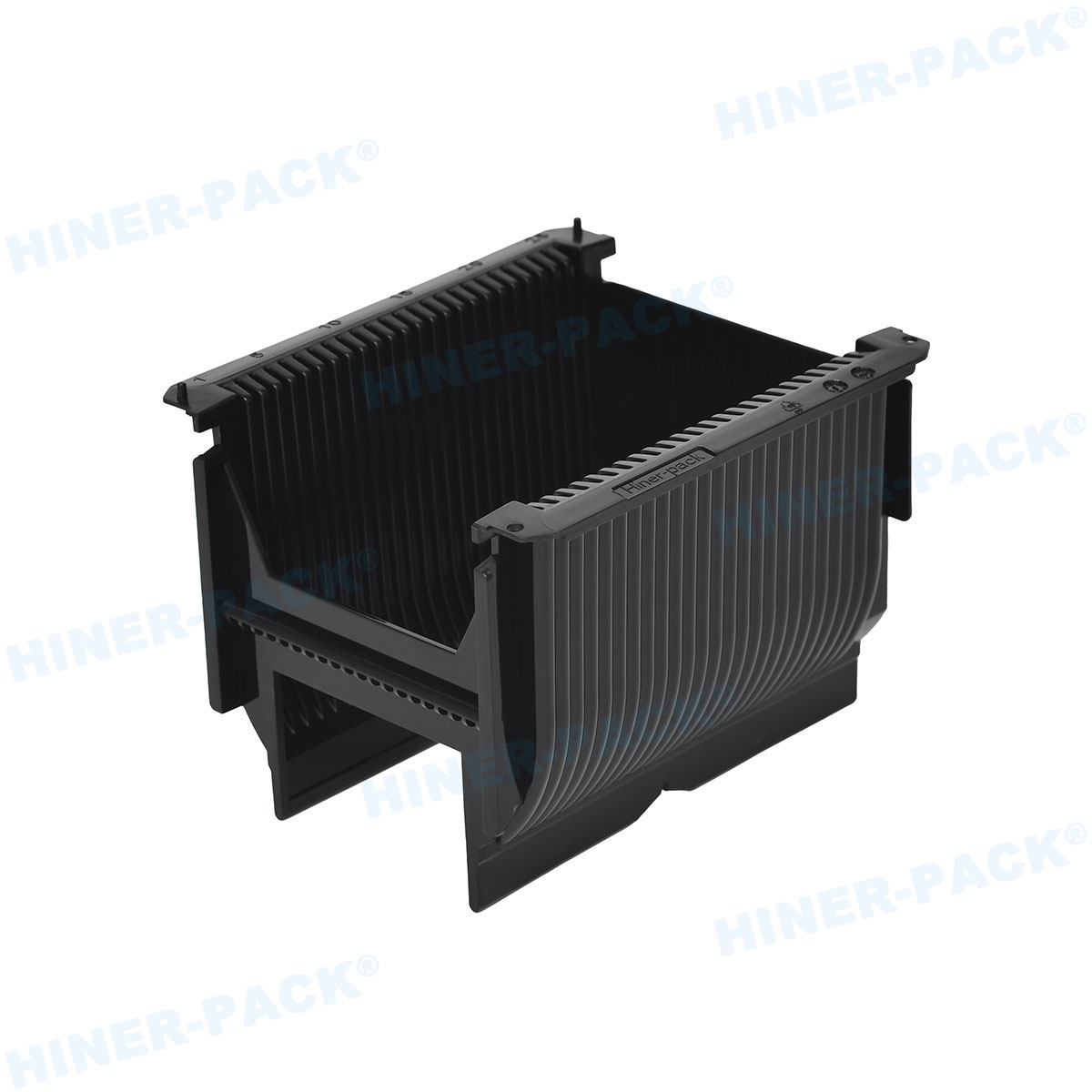
The Equipment Front End Module (EFEM) serves as the interface between wafer storage containers and process equipment, playing a crucial role in maintaining cleanliness and precision. Essentially, an Equipment Front End Module is a mini-environment that houses robots and aligners to transfer wafers from FOUPs to processing chambers without exposing them to external contaminants. This is especially important for 300mm wafer handling tools, where even microscopic particles can cause significant yield losses. A typical Equipment Front End Module includes components like load ports, pre-aligners, and robotic arms, all designed for high-speed, accurate wafer placement.
In the context of Advanced Wafer Handling Solutions, the EFEM has evolved to support higher throughput and flexibility. For instance, modern EFEMs can handle multiple wafer sizes and integrate with Automated Material Handling System networks for seamless material flow. Hiner-pack's innovations in Equipment Front End Module design focus on reducing footprint and energy consumption while enhancing reliability. Their modules often feature smart sensors that monitor wafer position and condition in real time, aligning with the demands of 450mm wafer handling research. By optimizing the Equipment Front End Module, manufacturers can achieve faster cycle times and better defect control, ultimately lowering production costs. This makes the EFEM a key element in the ecosystem of semiconductor wafer handling tools, bridging the gap between manual operations and full automation.
Advanced Wafer Handling Solutions by Hiner-pack
Hiner-pack has established itself as a global pioneer in Advanced Wafer Handling Solutions, offering a comprehensive portfolio that addresses the diverse needs of semiconductor fabs. Their products range from basic 300mm wafer handling tools to innovative systems geared toward 450mm wafer handling. What sets Hiner-pack apart is their focus on customization and integration, ensuring that their solutions work harmoniously with Automated Material Handling System and Equipment Front End Module setups. For example, their latest robotic handlers incorporate AI-driven vision systems to detect wafer defects during transfer, reducing scrap rates and improving quality assurance.
One notable offering from Hiner-pack is their line of Advanced Wafer Handling Solutions that emphasize sustainability, such as energy-efficient motors and recyclable materials. These solutions are designed to support the industry's shift toward greener manufacturing, without compromising on performance. In applications involving 450mm wafer handling, Hiner-pack's research teams are developing lighter, more durable handlers that can withstand the mechanical stresses of larger wafers. Additionally, their semiconductor wafer handling tools often include predictive maintenance features, which leverage IoT connectivity to alert operators to potential failures before they occur. By partnering with fabs worldwide, Hiner-pack continues to push the boundaries of what's possible, making Advanced Wafer Handling Solutions a catalyst for innovation in semiconductor production.
Future Trends in Wafer Handling Technology
The future of semiconductor wafer handling tools is shaped by trends like miniaturization, increased automation, and the adoption of larger wafer sizes. As the industry explores 450mm wafer handling, we can expect more collaborative efforts between companies like Hiner-pack and research institutions to overcome technical barriers. Key developments might include the use of magnetic levitation for contactless transport or advanced materials that reduce static electricity. Moreover, the integration of Automated Material Handling System with AI and machine learning will enable smarter decision-making, such as dynamic routing based on real-time fab conditions.
Another emerging trend is the focus on Advanced Wafer Handling Solutions that support heterogeneous integration, where multiple chip types are combined on a single wafer. This requires highly precise semiconductor wafer handling tools capable of handling diverse geometries and materials. Hiner-pack is actively investing in R&D to address these needs, with prototypes that offer greater flexibility and speed. Additionally, as environmental regulations tighten, future tools will likely emphasize energy efficiency and reduced carbon footprints. For instance, Hiner-pack's upcoming Equipment Front End Module designs aim to cut power consumption by 20% compared to current models. By staying ahead of these trends, the semiconductor industry can continue to drive progress in electronics, from smartphones to autonomous vehicles.
In summary, semiconductor wafer handling tools are indispensable to the semiconductor manufacturing ecosystem, enabling the precise and efficient movement of wafers through complex processes. From the widespread use of 300mm wafer handling tools to the promising potential of 450mm wafer handling, these technologies are evolving to meet higher demands for yield and scalability. Systems like the Automated Material Handling System and Equipment Front End Module play critical roles in automating and streamlining operations, while Advanced Wafer Handling Solutions from brands like Hiner-pack push the envelope with innovative features. As the industry advances, embracing these tools will be key to maintaining competitiveness and driving future growth. By investing in robust handling solutions, manufacturers can navigate challenges and capitalize on opportunities in the dynamic semiconductor landscape.
Frequently Asked Questions (FAQ)
Q1: What are the primary benefits of using 300mm wafer handling tools in semiconductor manufacturing?
A1: 300mm wafer handling tools offer several advantages, including higher throughput due to larger wafer sizes, which allow more chips to be produced per wafer. They also reduce manufacturing costs per unit and improve efficiency by integrating with automated systems like the Automated Material Handling System. Additionally, these tools are designed to minimize contamination and damage, leading to better yield rates in fabrication facilities.
Q2: How does 450mm wafer handling differ from 300mm, and what challenges does it present?
A2: 450mm wafer handling involves larger wafers (450mm in diameter) compared to the standard 300mm, potentially doubling chip output per wafer. However, it presents challenges such as increased wafer fragility, higher infrastructure costs, and the need for more robust semiconductor wafer handling tools to handle the weight and size. Technical hurdles include developing new materials and transport systems to prevent cracks and maintain cleanliness.
Q3: What role does an Automated Material Handling System play in a semiconductor fab?
A3: An Automated Material Handling System (AMHS) automates the transport of wafers between different stages of production, such as from storage to processing equipment. It enhances efficiency by reducing manual handling, minimizing contamination risks, and enabling real-time tracking and optimization. This system often works in tandem with Equipment Front End Module and Advanced Wafer Handling Solutions to ensure seamless material flow in modern fabs.
Q4: Can you explain the function of an Equipment Front End Module in wafer processing?
A4: An Equipment Front End Module (EFEM) acts as an interface between wafer storage containers (like FOUPs) and process tools, providing a controlled environment to transfer wafers without exposure to contaminants. It typically includes robotic arms, load ports, and alignment systems to ensure precise placement. This module is essential for maintaining high yields, especially when using 300mm wafer handling tools or exploring 450mm wafer handling, as it supports speed and accuracy in high-volume manufacturing.
Q5: How do Advanced Wafer Handling Solutions, such as those from Hiner-pack, improve semiconductor production?
A5: Advanced Wafer Handling Solutions, like those offered by Hiner-pack, enhance semiconductor production through innovations in robotics, AI, and material science. They improve precision, reduce defect rates, and increase throughput by integrating with systems such as the Automated Material Handling System and Equipment Front End Module. Hiner-pack's solutions also focus on sustainability and scalability, helping fabs adapt to future trends like 450mm wafer handling while maintaining cost-efficiency and reliability.
Q6: What future advancements can we expect in semiconductor wafer handling tools?
A6: Future advancements in semiconductor wafer handling tools may include greater adoption of AI for predictive maintenance, the development of contactless handling technologies like magnetic levitation, and enhanced integration with IoT for smarter fab management. As the industry moves toward 450mm wafer handling, we can also see more collaborations to address technical barriers, along with a focus on eco-friendly designs that reduce energy consumption and waste.


