In the high-precision environment of semiconductor fabrication, the journey
from the front-end-of-line (FEOL) to the back-end-of-line (BEOL) involves
numerous transport phases. Silicon wafers, the foundation of modern electronics,
are exceptionally fragile and susceptible to microscopic contamination. The
selection of a wafer
shippers manufacturer is therefore a decision that directly impacts
product yield and operational profitability. Professional-grade transport
solutions must provide more than just physical containment; they must serve as a
mobile cleanroom environment capable of mitigating mechanical stress,
electrostatic discharge (ESD), and chemical outgassing.
Engineering these containers requires a deep understanding of polymer science
and structural mechanics. As wafer diameters have increased to 300mm and
thicknesses have decreased for advanced 3D packaging, the technical requirements
for transport systems have become more stringent. Leading firms such as
[Hiner-pack] have
addressed these challenges by developing high-purity shipping solutions that
adhere to the most rigorous SEMI standards. This guide provides an in-depth
analysis of the technical benchmarks necessary to evaluate the capabilities of a
modern semiconductor packaging partner.
1. Material Science and ESD Protection Protocols
The primary concern for any wafer shippers
manufacturer is the selection of raw materials. The polymers used
must possess specific mechanical properties while maintaining a strict
electrical profile. Silicon is a semiconductor, and the buildup of static
electricity during transport can lead to Electrostatic Discharge events, which
can destroy sensitive circuitry or attract airborne molecular contaminants (AMC)
to the wafer surface.
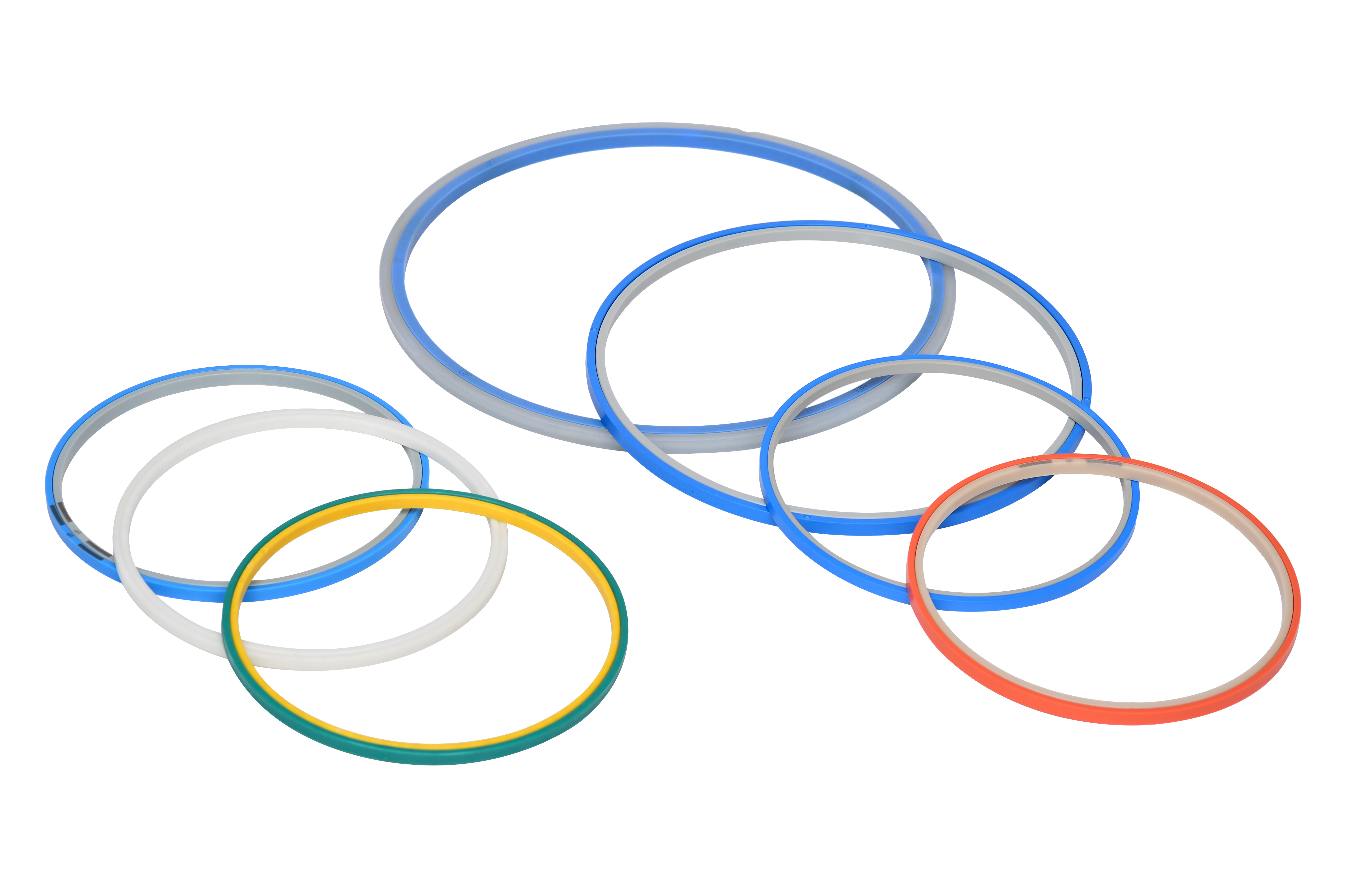
Surface Resistivity and Dissipative Properties
To prevent ESD, materials are typically infused with carbon fibers or
specialized anti-static agents to achieve a surface resistivity within the
dissipative range, generally between 10^4 and 10^11 ohms per square.
Carbon-filled Polypropylene (PP) or Polycarbonate (PC) are the industry
standards for their balance of rigidity and electrical performance. High-purity
PEEK (Polyetheretherketone) is often reserved for high-temperature applications
or environments where the lowest possible particle shed is mandatory.
Polymer Purity and Chemical Resistance
Beyond electrical properties, the material must be chemically inert. Shippers
are frequently exposed to cleaning agents and residual chemicals from the
fabrication process. A high-quality manufacturer ensures that the polymers do
not degrade or leach metallic ions when in contact with IPA (Isopropyl Alcohol)
or other common solvents. This chemical stability is fundamental for maintaining
the integrity of the wafers over long-duration international shipping
cycles.
2. Contamination Control and Outgassing Mitigation
The semiconductor industry operates at a scale where a single organic
molecule can cause a catastrophic failure in a transistor. A wafer shippers
manufacturer must therefore implement rigorous contamination
control measures during the production phase. This begins with manufacturing in
ISO Class 5 or Class 6 cleanrooms to ensure that the "as-shipped" particle count
is near zero.
Understanding Volatile Organic Compounds (VOCs)
Outgassing refers to the release of volatile gases from the plastic
components of the shipper. These gases can condense on the wafer surface,
creating a film that interferes with lithography or etching. Professional
suppliers utilize specialized vacuum-bake processes or select low-outgassing
resins to minimize Total Organic Carbon (TOC) levels. Testing for outgassing
involves sophisticated Gas Chromatography-Mass Spectrometry (GC-MS) to identify
and quantify trace amounts of phthalates, silicones, and other harmful
organics.
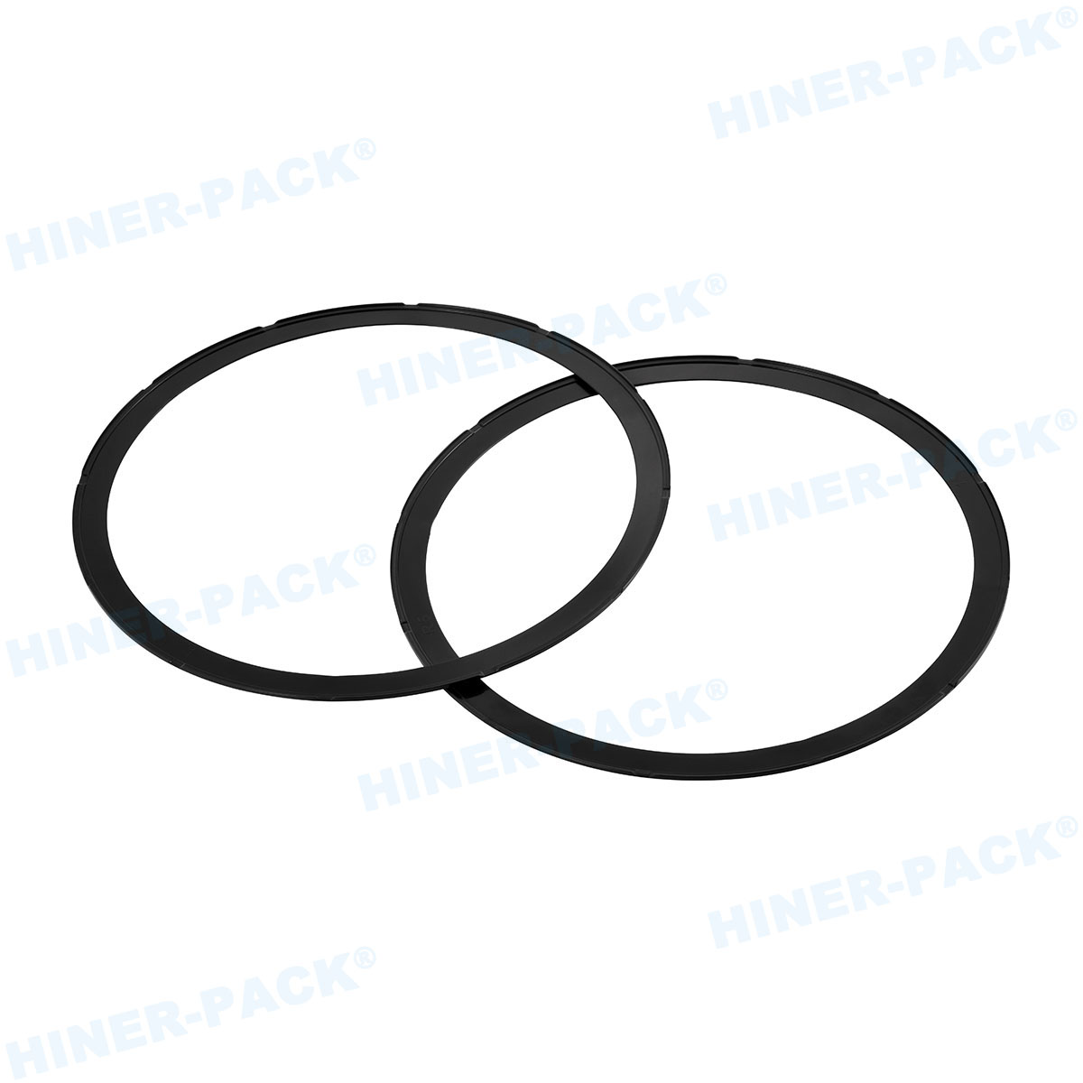
Sealing Technology and Particle Ingress
The interface between the shipper lid and the base must be engineered to
prevent the ingress of external particles. High-performance shippers utilize
high-purity elastomer gaskets or precision-machined "labyrinth" seals. These
designs ensure that even when subjected to the pressure changes of air freight,
the internal environment remains isolated from ambient pollutants.
3. Mechanical Stress and Vibration Dampening
During logistics, wafers are subjected to various mechanical forces,
including high-frequency vibrations and sudden shocks. A wafer shippers
manufacturer must design the internal architecture of the box to
absorb these forces without transferring them to the silicon substrate.
Coin-Stack vs. Vertical Configurations
For smaller wafers (100mm to 150mm), "coin-stack" shippers are common, where
wafers are layered horizontally with interleaf spacers. However, for 200mm and
300mm wafers, vertical shipping is often preferred to reduce the risk of
"bowing" or structural fracture. The "wafer cushions" or "retainers" located at
the top and bottom of the container are designed with specific spring constants
to provide a secure grip while allowing for enough flex to dampen kinetic
energy.
G-Force Resilience Testing
Advanced manufacturers subject their designs to rigorous drop tests and
vibration table simulations. These tests measure the G-forces experienced by a
dummy wafer inside the container. By optimizing the geometry of the wafer slots
and the thickness of the outer shell, companies like [Hiner-pack] can guarantee that
wafers remain intact even under the harshest transport conditions. This
structural engineering is particularly vital for thinned wafers, which have
significantly lower fracture toughness.
4. SEMI Standards and Automation Compatibility
In a modern "Lights Out" fab, human contact with wafers is non-existent. All
transport containers must be compatible with Automated Material Handling Systems
(AMHS). This requires the wafer shippers
manufacturer to adhere strictly to SEMI (Semiconductor Equipment
and Materials International) standards.
SEMI M1 and M12 Compliance
These standards dictate the precise dimensions, notch orientations, and
fiducial markings required for automation. A shipper that deviates from these
measurements by even a fraction of a millimeter can cause a tool jam, leading to
significant downtime. High-end shipping boxes, such as FOSBs (Front Opening
Shipping Boxes), must feature precision-engineered kinematic couplings and
robotic lifting flanges that allow for seamless handoffs between overhead hoist
transports (OHT) and stockers.
Identification and Tracking
Modern shippers often integrate RFID (Radio Frequency Identification) tags or
high-contrast laser-etched barcodes. This allows for real-time lot tracking
throughout the global supply chain. The integration of these tracking elements
must be done in a way that does not introduce new contamination risks or
interfere with the box’s ESD shielding.
5. Specialized Solutions for Thin and Fragile Wafers
The rise of Heterogeneous Integration (HI) and Fan-Out Wafer-Level Packaging
(FOWLP) has led to the widespread use of wafers thinned to less than 100
microns. These wafers are prone to warping and "potato chipping." A specialized
wafer shippers
manufacturer must provide solutions tailored to these fragile
substrates.
Taiko Wafer Support: Specialized shippers that accommodate
the thicker outer ring of Taiko wafers while protecting the thinned inner
area.
Interleaf Materials: The use of non-woven, lint-free, and
anti-static interleaf discs to prevent surface-to-surface contact in coin-stack
configurations.
Vacuum-Compatible Designs: Some advanced wafers must be
shipped under vacuum or in an inert nitrogen environment. This requires shippers
with integrated valves and high-integrity hermetic seals.
6. Application Scenarios Across the Semiconductor Lifecycle
The requirements for wafer transport vary significantly depending on the
stage of production and the end-user requirements. A versatile manufacturer must
offer a catalog that spans the entire lifecycle.
Ingot-to-Wafer Transport
Initial silicon wafers, post-sawing and polishing, require bulk transport
solutions. These are often high-capacity "cassette-in-box" designs that
prioritize volume efficiency and basic protection. The focus here is on
preventing surface scratches during the transition from the wafering house to
the fab.
In-Process Fab Inter-Bay Transport
Within the fab, wafers move between different tool sets (photolithography,
ion implantation, CMP). This requires FOUPs (Front Opening Unified Pods) that
are designed for high-frequency robotic access and are often integrated with
nitrogen purging systems to prevent the oxidation of copper layers between
process steps.
Global Logistics and Foundry-to-OSAT Shipping
When completed wafers are sent from a foundry to an Outsourced Semiconductor
Assembly and Test (OSAT) provider, the shipping container becomes the final line
of defense against the external world. These shippers must be rugged enough for
international air freight while maintaining the internal purity levels achieved
in the cleanroom. [Hiner-pack] specializes in
these high-reliability shipping solutions, ensuring that the value added during
the fabrication process is not lost during transit.
The role of a wafer
shippers manufacturer extends far beyond simple plastic molding. It
is a discipline that combines advanced material science, precision mechanical
engineering, and rigorous contamination control. As the semiconductor industry
moves toward smaller process nodes and more complex 3D architectures, the
importance of secure, high-purity transport will only increase.
Choosing the right partner requires a thorough evaluation of their cleanroom
capabilities, their adherence to SEMI standards, and their ability to provide
specialized solutions for thinned and fragile wafers. By focusing on these
technical benchmarks, B2B procurement and engineering teams can ensure that
their silicon assets are protected throughout the global supply chain,
ultimately safeguarding their yield and brand reputation in a highly competitive
market.
Frequently Asked Questions
Q1: What is the typical shelf life of a wafer shipper's ESD
properties?
A1: For shippers using permanent carbon-filled polymers, the ESD properties
are typically as long-lived as the plastic itself. However, for shippers
utilizing topical anti-static coatings, the properties may degrade after 6-12
months or after multiple cleaning cycles. It is recommended to verify surface
resistivity periodically.
Q2: Can wafer shippers be reused, and what is the
protocol?
A2: Yes, many shippers are designed for multiple cycles. However, they must
undergo a validated aqueous cleaning process in a cleanroom environment to
remove accumulated particles and organic residues. The number of reuses depends
on the wear of the mechanical retainers and the stability of the polymer.
Q3: How does outgassing affect the wafer during long-term
storage?
A3: Long-term storage (over 3 months) in a high-outgassing container can lead
to "haze" on the wafer surface. This haze is actually a thin layer of condensed
organic compounds that can cause adhesion failures in subsequent processing
steps. Low-outgassing materials are mandatory for long-term storage.
Q4: What is the difference between a FOUP and a FOSB?
A4: A FOUP (Front Opening Unified Pod) is primarily used for internal fab
transport and is designed to interface directly with process tools. A FOSB
(Front Opening Shipping Box) is designed for external shipping between
facilities; it often lacks some of the complex internal mechanisms of a FOUP but
offers superior mechanical protection for logistics.
Q5: Why is Polycarbonate (PC) often preferred over Polypropylene (PP)
for 300mm shippers?
A5: Polycarbonate offers superior dimensional stability and rigidity. For
300mm wafers, the weight and size require a container that will not flex or
warp, as even slight deformations can interfere with robotic sensors and
kinematic couplings. PC also tends to have lower outgassing profiles for certain
organic species.
Are you seeking a technical partner for your semiconductor packaging
and transport needs?
At Hiner-pack, we understand the high stakes of semiconductor logistics. Our
engineering team is dedicated to providing high-purity, SEMI-compliant shipping
solutions that protect your technological investments. Whether you require
custom inserts for thinned wafers or high-volume FOSB solutions, we have the
expertise to deliver. Contact us today to discuss your specific technical
requirements and learn how we can optimize your transport yield.
[For professional inquiries and customized technical quotations,
please reach out to our global support team. Inquiry Now!]


