The semiconductor industry operates at the threshold of physical possibility,
where features are measured in nanometers and purity is defined by parts per
trillion. In this context, the infrastructure of the supply chain is just as
vital as the lithography tools themselves. A wafer shippers
factory serves as a high-precision manufacturing node,
responsible for producing the protective environments that house silicon wafers
during international transit and internal fab movement. These containers are not
merely plastic boxes; they are sophisticated instruments designed to prevent
contamination, mitigate mechanical shock, and ensure compatibility with advanced
robotic handling systems.
For B2B procurement managers and packaging engineers, the choice of a
manufacturing partner involves a rigorous audit of technical capabilities. The
transition toward larger wafer sizes and thinner substrates has placed immense
pressure on packaging providers to innovate. Leading organizations such as
[Hiner-pack] have responded by integrating advanced polymer science with automated cleanroom
production. This article examines the technical benchmarks that define
excellence in the production of wafer transport solutions, from the molecular
level of the raw materials to the mechanical tolerances of the finished
product.
1. Cleanroom Manufacturing Infrastructure
The core of a high-performance wafer shippers
factory is its controlled environment. Because wafer shippers
are used in the most sensitive areas of a semiconductor fab, they must be
produced in an environment that matches or exceeds the cleanliness of the
end-user's facility. A standard factory layout often separates the high-heat
injection molding process from the final assembly and packaging phases.
ISO Class 5 and 6 Integration
Modern production lines utilize ISO Class 5 (Class 100) or Class 6 cleanrooms
for the assembly of Front Opening Shipping Boxes (FOSB) and Front Opening
Unified Pods (FOUP). This ensures that no airborne particulates are trapped
inside the container during the sealing process. High-efficiency particulate air
(HEPA) filtration systems must maintain constant laminar flow over the assembly
stations, and the air change rates must be monitored continuously to prevent the
accumulation of microscopic debris.
Automated Molding Environments
Precision injection molding for wafer carriers requires a stable ambient
environment to ensure dimensional consistency. Variations in temperature or
humidity during the molding process can cause slight warpage in the plastic,
leading to failures in robotic automation interfaces. Advanced factories utilize
closed-loop feedback systems on their molding machines to adjust for
environmental fluctuations in real-time, ensuring that every unit produced meets
the exact mechanical specifications required by SEMI standards.
2. Advanced Polymer Science and Outgassing Mitigation
The choice of material determines the protective capability of the shipper. A
wafer shippers
factory must possess the expertise to work with
high-performance engineering plastics, each chosen for its specific chemical and
physical properties.
Polycarbonate (PC): Known for its high impact resistance
and dimensional stability. It is the industry standard for 300mm FOSB shells,
providing a rigid frame that protects against physical deformation.
Polyetheretherketone (PEEK): Utilized for wafer-contact
components such as teeth and retainers. PEEK offers exceptional wear resistance
and is capable of withstanding the high temperatures associated with certain fab
processes without degrading.
Carbon-Fiber Additives: These are integrated into the
polymer matrix to provide permanent electrostatic discharge (ESD) protection,
ensuring that the surface resistivity remains within the dissipative range (10^4
to 10^10 ohms/sq).
One of the most crucial technical hurdles in material selection is the
management of Airborne Molecular Contaminants (AMC). Volatile organic compounds
(VOCs) can outgas from the plastic and condense on the wafer surface, causing
"haze" and affecting lithography yields. Professional manufacturers utilize
vacuum-drying protocols and low-outgassing resins to ensure that the total
organic carbon (TOC) levels remain within acceptable industry limits.
3. Precision Mechanical Design and SEMI Compliance
In a modern automated fab, a wafer shipper is more than a container; it is a
robotic interface. Compliance with SEMI (Semiconductor Equipment and Materials
International) standards is the most important requirement for any wafer shippers
factory. These standards, such as SEMI M1 and E15.1, define the
precise dimensions for kinematic couplings, robotic flanges, and wafer slot
spacing.
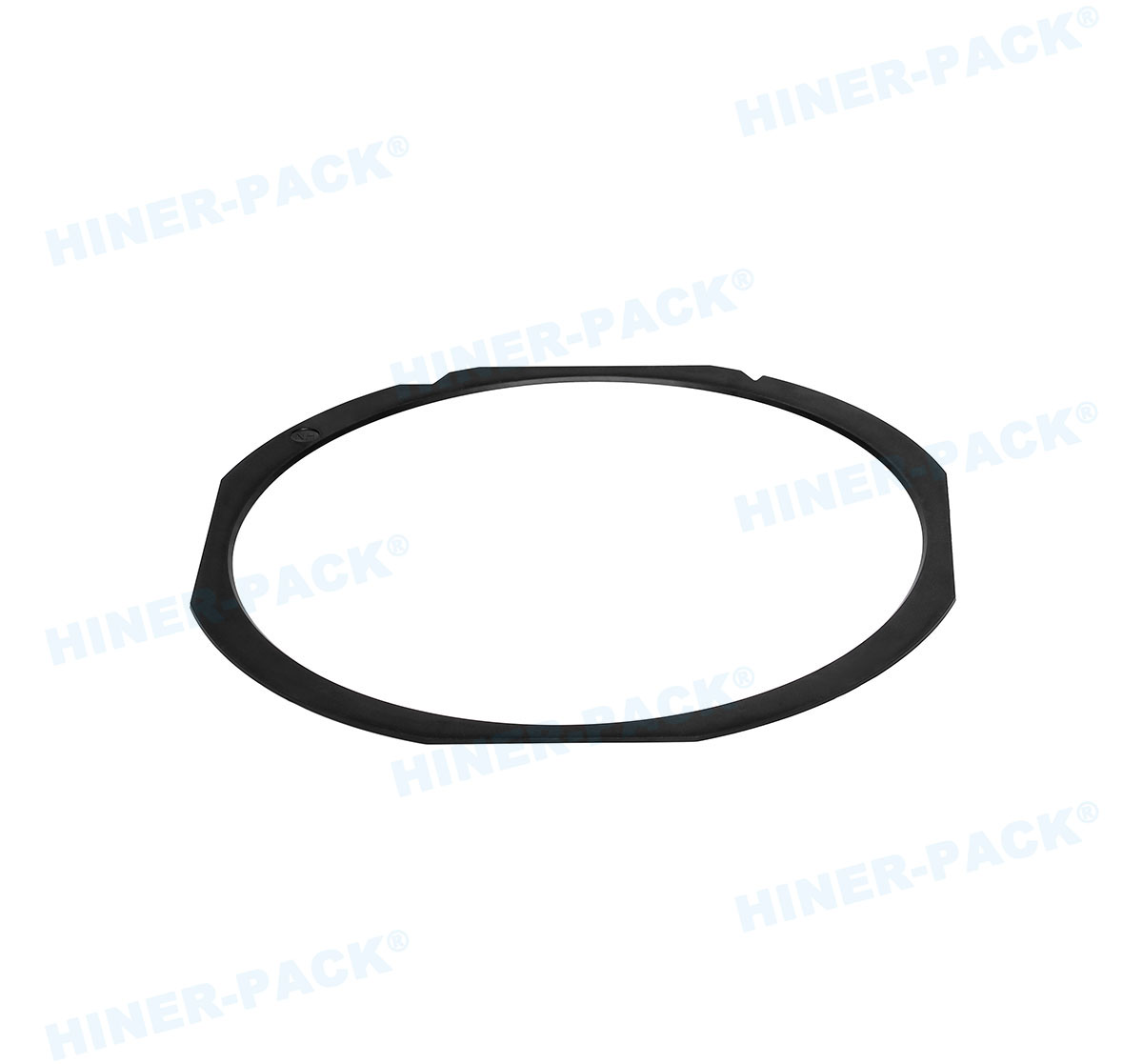
Kinematic Coupling Accuracy
The three-point kinematic coupling at the base of a FOUP or FOSB must be
manufactured with sub-millimeter precision. This interface allows a robotic load
port to "know" the exact position of the container. Any deviation in the molding
of these points can result in a robotic mispick, leading to shattered wafers and
massive financial losses. Quality control in the factory involves using
Coordinate Measuring Machines (CMM) to verify the geometric tolerances of every
batch.
Wafer Constraint Systems
The internal "teeth" or slots that hold the wafers must provide a secure grip
without exerting excessive force. As wafers have become thinner (down to 50
microns in some cases), the design of the wafer retainer must account for
substrate "bowing." Modern factory designs use sophisticated simulation software
to model the stress distribution on the wafer edges, ensuring that the shipping
box can withstand G-forces during air freight without inducing fractures.
4. Moisture Control and Hermetic Sealing Technology
Environmental factors such as humidity can be detrimental to wafer integrity,
particularly for those with sensitive copper layers or advanced low-k
dielectrics. A specialized wafer shippers
factory integrates high-performance sealing technology into its
product designs.
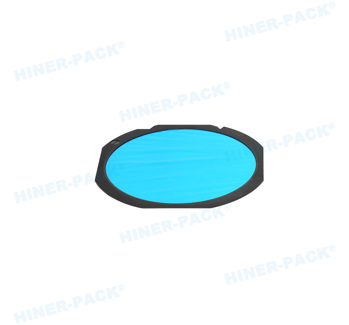
Gasket Engineering
Advanced shipping boxes utilize high-purity elastomer gaskets that provide a
hermetic seal. These gaskets must remain flexible over a wide range of
temperatures and be resistant to compression sets. The factory must ensure that
the gasket is bonded to the frame in a way that prevents "particle traps" at the
interface. [Hiner-pack] focuses on
the integrity of these seals to ensure that the internal environment remains at
the specified humidity level throughout the shipping cycle.
Nitrogen Purge Capabilities
For FOUPs used in-process, the ability to maintain an inert environment is a
requirement. The factory must integrate precision-machined purge valves into the
container base. These valves allow the fab's internal system to flush the
container with nitrogen, displacing oxygen and moisture. Testing these valves
for leak rates and particulate generation is a fundamental part of the factory's
quality assurance protocol.
5. Rigorous Quality Assurance and Validation Protocols
The path from a raw polymer pellet to a finished FOSB is governed by a
complex validation stack. A professional manufacturer does not rely on visual
inspection alone; they utilize a suite of analytical tools to verify
performance.
Particle Testing: Using liquid particle counters (LPC) to
measure the cleanliness of the container's interior surfaces.
Impact and Vibration Testing: Simulating the rigors of
global logistics using vibration tables and drop testers to ensure the wafers
remain secure.
Chemical Resistance: Verifying that the shippers can
withstand repeated cleaning cycles with Isopropyl Alcohol (IPA) or specialized
detergents without losing structural integrity.
ESD Verification: Measuring surface resistance at multiple
points on the box to ensure consistent dissipative performance.
This level of verification is what ensures that the "yield integrity" of the
silicon wafers is maintained. When a B2B client audits a wafer shippers
factory, they are looking for documented evidence that these
tests are performed on every production lot, not just on prototypes.
6. Solving Industry Pain Points: The Fragility of Thinned Wafers
As the semiconductor industry moves toward 3D stacking and advanced
packaging, wafers are being ground to extreme thinness. These substrates are
significantly more fragile than standard 775-micron wafers. The industry pain
point here is the high rate of breakage during transport between foundries and
OSAT (Outsourced Semiconductor Assembly and Test) providers.
The solution provided by advanced factories involves specialized "low-stress"
wafer cushions. These cushions utilize softer polymers and more complex
geometries to distribute the clamping force over a larger area of the wafer
edge. Furthermore, the factory must ensure that the interleaf materials (if used
in coin-stack shippers) are completely lint-free and anti-static to avoid
introducing new contaminants to the thinned surface. By focusing on these
specific technical challenges, manufacturers can help their clients achieve
higher final yields.
7. Supply Chain Resilience and Global Logistics Support
The semiconductor market is characterized by rapid cycles of demand. A
factory's ability to scale production while maintaining quality is a major
competitive advantage. This requires a robust supply chain for raw materials,
ensuring that only certified, high-purity resins are used.
Moreover, the factory must understand the logistics requirements of its
clients. This includes providing specialized secondary packaging that meets
international shipping regulations and ensures that the cleanroom-packed
shippers do not become contaminated during the "last mile" of delivery.
Organizations like [Hiner-pack] leverage
their proximity to global shipping hubs and their deep understanding of fab
logistics to provide a seamless experience for B2B customers across the
globe.
8. Sustainability and Lifecycle Management
The high volume of plastic used in semiconductor packaging has led to a
growing focus on sustainability. A forward-thinking wafer shippers
factory is now exploring ways to reduce environmental impact
without compromising purity. This includes the development of reusable shipping
systems and the implementation of recycling programs for end-of-life containers.
While the reuse of shippers in a Class 1 fab is limited by strict purity
requirements, many components can be recycled for use in less sensitive
applications, reducing the overall environmental footprint of the industry.
Lifecycle management also involves helping clients manage the "aging" of
their shippers. Over time, plastic can become brittle and ESD properties can
drift. A professional manufacturer provides guidelines for the inspection and
retirement of older units, ensuring that a degraded box never compromises a
valuable lot of wafers.
Engineering a high-performance wafer shippers
factory is an exercise in technical discipline. From the
micron-level control of airborne particulates to the precise chemical
formulation of ESD-safe polymers, every aspect of the manufacturing process must
be optimized for safety and reliability. As the semiconductor industry continues
to push the boundaries of what is possible, the role of specialized packaging
will remain a cornerstone of successful global production.
By prioritizing SEMI compliance, investing in advanced molding technology,
and maintaining rigorous cleanroom standards, a world-class factory provides the
security that global foundries and assembly houses require. In the competitive
world of semiconductor fabrication, where yield is the most important metric,
the integrity of the transport system is not an option—it is a fundamental
requirement for success.
Frequently Asked Questions
Q1: What ISO cleanroom class is required for a wafer shippers
factory?
A1: For the assembly and final packaging of 300mm FOSBs and FOUPs, ISO Class
5 (Class 100) or Class 6 is the industry standard. The molding areas may operate
at a lower class, but the final integration of components must occur in a highly
controlled environment to prevent particle entrapment.
Q2: Why is the dimensional stability of a wafer shipper so important
for automation?
A2: Automated Material Handling Systems (AMHS) and robotic load ports rely on
precise coordinates to pick and place wafers. If a shipper warps even by a
fraction of a millimeter due to poor molding in the factory, the robot may
collide with the wafer or the container, causing catastrophic breakage.
Q3: How does a factory ensure that ESD protection is
permanent?
A3: Permanent ESD protection is achieved by compounding conductive or
dissipative additives (like carbon fiber or specialized polymers) directly into
the plastic resin before injection molding. This is superior to topical
anti-static sprays, which can wear off or contaminate the wafers.
Q4: What is the role of outgassing testing in the manufacturing
process?
A4: Outgassing testing verifies that the volatile organic compounds (VOCs)
released by the plastic are below a certain threshold. This is vital because
these gases can condense on the wafers, leading to chemical contamination that
interferes with sensitive manufacturing steps like atomic layer deposition
(ALD).
Q5: Can wafer shippers be customized for specific thinned wafer
requirements?
A5: Yes, a professional factory can customize the internal wafer retainers
and cushions to provide specific clamping forces. This is often necessary for
Taiko wafers or ultra-thin substrates where standard shipping boxes might apply
too much pressure on the edges.
Are you looking for a technical partner to secure your wafer
transport yield?
At Hiner-pack, we understand the complex requirements of modern semiconductor
logistics. Our state-of-the-art manufacturing facility is designed to meet the
highest industry standards for purity, precision, and reliability. Whether you
are managing the transition to advanced nodes or seeking robust solutions for
international wafer shipping, our engineering team is here to support you.
Contact us today for a technical consultation or a customized project
quotation.
[For expert support and high-performance wafer transport solutions,
please reach out to our technical sales team. Inquiry Now!]


