
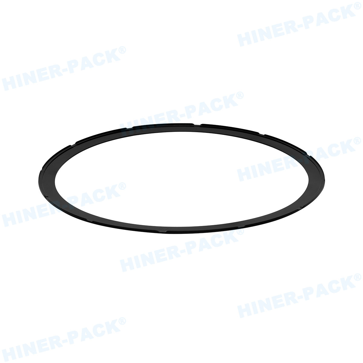
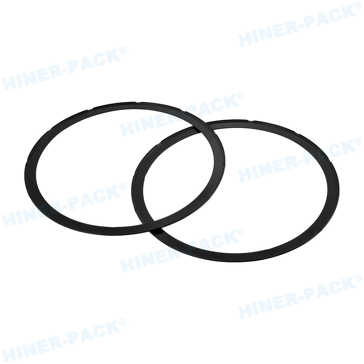
In semiconductor back-end manufacturing, the wafer film frame ring is a silent workhorse. It supports the wafer during dicing, die sorting, and pick-and-place operations. A substandard ring causes wafer warpage, tape wrinkling, and die shift—directly reducing yield.
This article provides six measurable specifications for evaluating any film frame ring. We cover material properties, dimensional tolerances, surface finish, and reusability protocols. Each parameter includes industry benchmarks from SEMI standards and practical cleanroom data.
Hiner-pack supplies wafer film frame rings that meet Class 10 cleanroom requirements and survive 500+ autoclave cycles. Let's examine the engineering details.
1. Material Selection: Stainless Steel vs. Engineered Plastics
Film frame rings are typically manufactured from two material families: austenitic stainless steel (SUS304 or SUS316) or high-performance polymers (PEEK, PPS, or carbon-fiber reinforced ABS).
Stainless steel rings: Provide high rigidity and thermal stability (CTE ~17 ppm/°C). Ideal for large-diameter wafers (300mm) and processes with elevated temperatures (up to 150°C). Susceptible to scratching and require passivation.
Plastic rings: Lightweight (40% less mass than steel), ESD-safe with surface resistivity 10⁶–10⁹ Ω/sq, and non-marring. Suitable for manual handling and automated equipment. Lower modulus may cause flexing under high tape tension.
For a wafer film frame ring used in high-volume die attach, specify SUS304 with electropolished finish. For test or R&D environments, PEEK rings offer chemical resistance to dicing coolants.
2. Dimensional Standards: SEMI G73 and Industry Variants
Film frame rings follow standard outer diameters (OD) and inner diameters (ID) defined by SEMI G73 for 200mm and 300mm wafers. Common sizes:
6-inch (150mm) wafer: OD 186–190 mm, ID 156–160 mm, thickness 1.5–2.0 mm.
8-inch (200mm) wafer: OD 240–250 mm, ID 210–216 mm, thickness 2.0–2.5 mm.
12-inch (300mm) wafer: OD 380–400 mm, ID 330–340 mm, thickness 3.0–4.0 mm.
Flatness tolerance for the ring mounting surface should be ≤ 0.1 mm across the entire circumference. Deviations cause uneven tape adhesion and wafer stress. Request a CMM report for each batch.
Some equipment suppliers (Disco, Tokyo Seimitsu) have proprietary ring designs. Always verify compatibility with your dicing saw chuck table and tape mounter.
3. Surface Finish and Particle Generation
In cleanroom environments (ISO Class 5 or better), the wafer film frame ring must not shed particles. Surface roughness (Ra) should be ≤ 0.4 μm for steel rings, and ≤ 0.8 μm for plastic rings.
Particle performance test per SEMI F73:
After ultrasonic cleaning in DI water, particle counts (≥0.3 μm) shall be ≤ 10 particles per cm².
Ionic contamination: ≤ 0.1 μg/cm² of chloride, sodium, or potassium.
Hiner-pack provides third-party test reports for every ring batch. For stainless steel rings, electropolishing reduces particle generation by 90% compared to mechanical polishing.
4. Compatibility with Dicing Tapes (UV and Non-UV)
The ring's inner and outer lips must securely grip the dicing tape without cutting or delaminating. Tape adhesion strength to the ring flange is measured by 90° peel test (ASTM D3330).
Key design features:
Radiused edges (R0.2–0.5 mm) to prevent tape tearing under tension.
Retention groove or serration on the outer flange for UV tape after curing.
Alignment marks (laser-etched) for automated tape mounter orientation.
For UV-curable tapes, the ring material should not absorb UV wavelengths (365 nm). PEEK and stainless steel have excellent UV resistance; some ABS grades yellow and become brittle.
Test tape adhesion after thermal cycling (25°C → 85°C → 25°C, 10 cycles). Tape lift-off should be zero. If lift exceeds 2 mm, the ring surface energy is too low—treat with plasma or corona.
5. Reusability and Cleaning Protocols
Many fabs reuse film frame rings to reduce consumable costs. A reusable wafer film frame ring must withstand repeated chemical cleaning and autoclaving without degradation.
Recommended cleaning process:
Pre-rinse with deionized water (18 MΩ·cm).
Ultrasonic immersion in 2% alkaline detergent (pH 11) at 50°C for 10 minutes.
Triple rinse with DI water, then IPA vapor drying.
Inspection under 20x magnification for residual particles or corrosion.
Stainless steel rings survive 500+ cleaning cycles. Plastic rings typically last 100–200 cycles before surface roughening increases particle shedding. Wafer processing accessories suppliers offer ring refurbishment services including re-passivation and flatness re-certification.
6. ESD Control and Surface Resistivity
Electrostatic discharge (ESD) can damage sensitive devices during die attach and wire bonding. The film frame ring must provide a controlled path to ground.
Specifications per ANSI/ESD S20.20:
Surface resistivity: 10⁵ to 10⁹ Ω/sq for static dissipative plastics.
Volume resistivity: ≤ 10⁹ Ω·cm.
Charge decay time (from 1000V to 100V): less than 2 seconds at 50% RH.
Stainless steel rings are conductive (surface resistivity < 10³ Ω/sq) and require grounding clips on the dicing chuck. Plastic rings with carbon fiber filler achieve stable ESD performance without metal contact.
Measure surface resistivity using a concentric ring probe (ASTM D257). Avoid rings with sprayed-on anti-static coatings—they wear off after 20 cleaning cycles.
Frequently Asked Questions (FAQ)
Q1: What is the typical lifespan of a stainless steel wafer film frame ring in high-volume production?
A1: With proper cleaning and handling, SUS304 rings last 3–5 years or 2,000–3,000 cycles. Replacement is needed when flatness exceeds 0.15 mm, or when visible pitting corrosion appears. Hiner-pack offers a flatness recertification service to extend ring life by 12 months.
Q2: Can I use a 200mm wafer film frame ring for 150mm wafers with an adapter?
A2: Yes, but only with a precision adapter ring that centers the smaller wafer. The adapter must have the same thickness as the standard ring flange to maintain tape tension. However, many dicing saws require specific ring OD for chuck clamping. Check your equipment manual. Using an incorrect ring may void the warranty.
Q3: How do I verify the flatness of a delivered batch of film frame rings?
A3: Place the ring on a granite surface plate (grade AA or better) and measure the gap with a feeler gauge or dial indicator at 8 equally spaced points. Maximum deviation should be ≤ 0.1 mm. For high-precision applications (e.g., thin wafer handling), specify ≤ 0.05 mm and request a CMM report from the supplier.
Q4: What causes tape wrinkling on the film frame ring during mounting?
A4: Three common causes: 1) Uneven ring flatness (>0.1 mm) causing non-uniform tape tension; 2) Improper tape mounter roller pressure (should be 2–3 N/mm); 3) Residual adhesive on the ring flange from previous use. Clean the flange with isopropyl alcohol and a lint-free wipe before each mounting.
Q5: Are there industry standards for marking wafer film frame rings with barcodes or RFID?
A5: Yes. SEMI T7 specifies 2D data matrix symbol placement (5 mm × 5 mm) on the ring outer edge. Some fabs use RFID tags embedded in the plastic ring. For stainless steel rings, laser etching is permanent and withstands cleaning. Hiner-pack's product line includes pre-engraved rings with barcode and RFID options.
Ready to Source High-Performance Wafer Film Frame Rings?
Selecting the right wafer film frame ring impacts dicing yield, equipment uptime, and cleanroom consumables cost. Generic rings often fail flatness specifications or shed particles after a few cleaning cycles.
Contact the engineering team at Hiner-pack for a free material consultation. Provide your wafer size (150/200/300 mm), process temperatures, cleaning frequency, and tape type. We will return a detailed specification sheet, test report sample, and pricing for trial batches within 5 business days.
Send your inquiry now: https://www.waferboxes.com/contact.html – or request a sample kit for cleanroom evaluation.


