
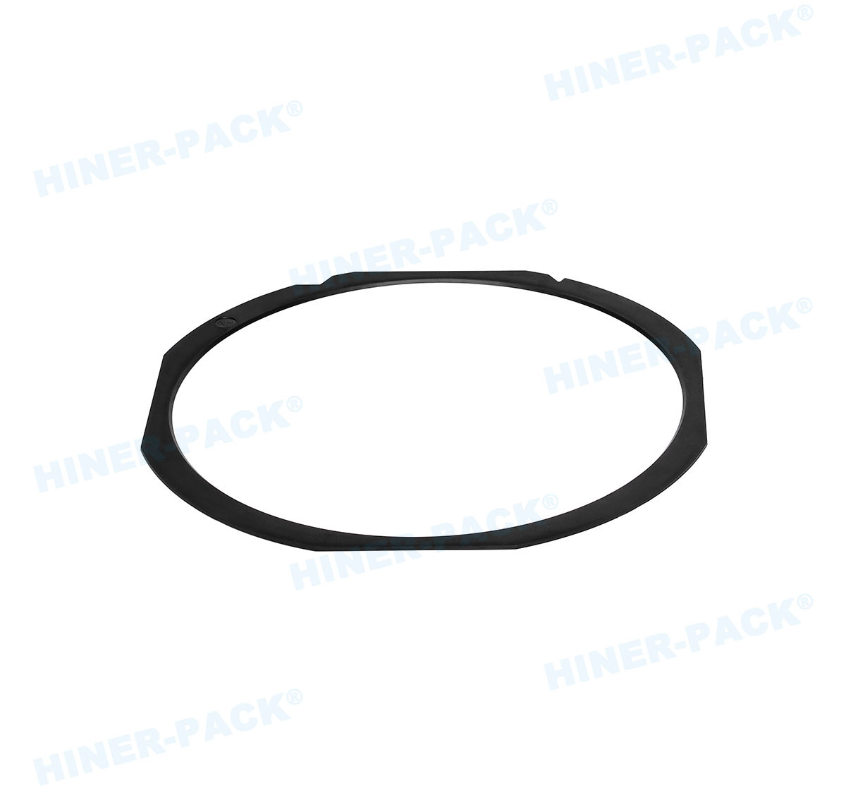
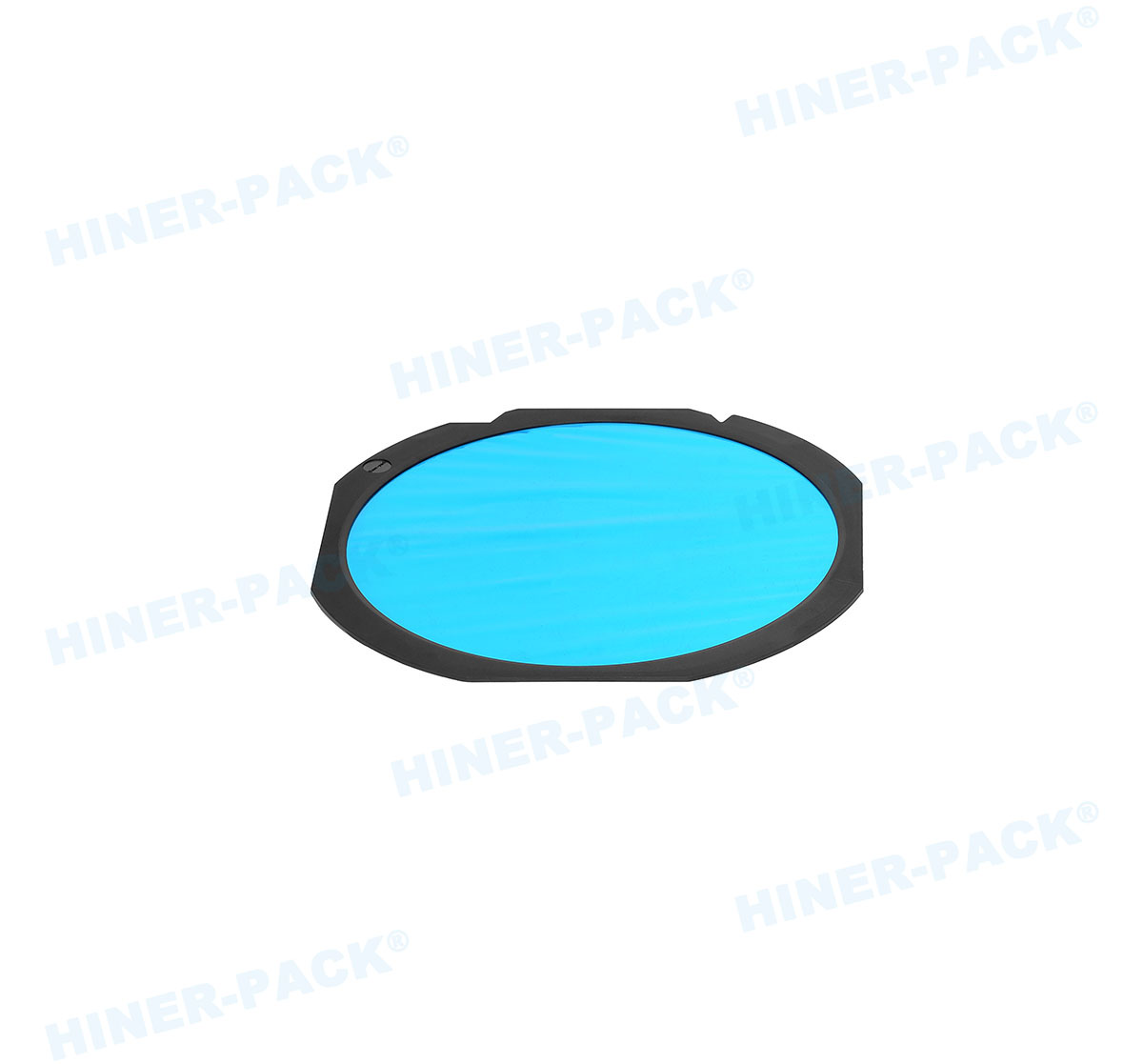
The wafer dicing frame ring is a precision component that directly impacts die shift, saw quality, and pick-and-place efficiency. A poorly designed ring causes tape delamination, coolant ingress, and broken dies—each reducing overall equipment effectiveness (OEE).
This article defines eight quantifiable metrics for evaluating any dicing frame ring. We examine material stiffness, dimensional stability, surface finish, and compatibility with automatic taping and dicing equipment. All parameters reference SEMI standards and cleanroom validation data.
Hiner-pack manufactures wafer dicing frame rings that sustain <0.05 mm flatness after 1,000 cleaning cycles. Let's review the engineering criteria.
1. Ring Flatness and Warpage Control
Flatness is the most critical attribute for a wafer dicing frame ring. Any deviation transfers stress to the wafer during tape mounting and saw chuck clamping.
Acceptable flatness per SEMI G73:
Standard grade: ≤ 0.1 mm total indicator reading (TIR) across the mounting flange.
Precision grade (thin wafers <150 μm): ≤ 0.05 mm TIR.
Measurement method: Place ring on a granite surface plate (grade AA) and scan with a dial indicator at 12 points.
Warpage exceeding 0.1 mm leads to uneven tape tension, causing die shift during dicing. Request a flatness certificate with every batch. Hiner-pack provides laser interferometry data for each ring.
2. Material Composition and Thermal Stability
Dicing frame rings are exposed to cooling water, dicing spindle vibrations, and UV curing lamps. Two material families dominate:
Stainless steel (SUS304 / SUS316): Coefficient of thermal expansion (CTE) 17 ppm/°C. Suitable for high-speed dicing (60,000 rpm spindles). Resists coolant corrosion but adds mass.
PEEK or PPS composites: CTE 25–30 ppm/°C. Lightweight, chemical resistant, and ESD-safe. May flex under high tape tension (50 N or more).
For 300mm wafers with ultra-thin dies, stainless steel rings provide better vibration damping. For manual assembly lines, plastic rings reduce operator fatigue.
3. Surface Finish and Particle Shedding
In ISO Class 5 cleanrooms, the wafer dicing frame ring must not contaminate the dicing area. Surface roughness (Ra) limits:
Steel rings (electropolished): Ra ≤ 0.2 μm.
Plastic rings (machined or molded): Ra ≤ 0.6 μm.
Particle generation test per SEMI F73:
Immerse ring in DI water, ultrasonic agitate for 5 minutes.
Count particles ≥0.3 μm: ≤ 20 particles per cm².
Ionic contamination: Chloride ≤ 0.05 μg/cm², sodium ≤ 0.1 μg/cm².
Semiconductor processing accessories suppliers often skip electropolishing on steel rings, resulting in 10x higher particle counts. Always request an independent cleanliness report.
4. Dimensional Accuracy: OD, ID, and Thickness Tolerances
Standard dicing frame ring sizes for different wafer diameters:
150mm (6-inch) wafer: OD 186.0 ±0.1 mm, ID 156.0 ±0.1 mm, thickness 1.8 ±0.05 mm.
200mm (8-inch) wafer: OD 245.0 ±0.1 mm, ID 212.0 ±0.1 mm, thickness 2.0 ±0.05 mm.
300mm (12-inch) wafer: OD 395.0 ±0.15 mm, ID 340.0 ±0.15 mm, thickness 3.0 ±0.05 mm.
Match these dimensions to your dicing saw chuck table and tape mounter. Disco and Tokyo Seimitsu machines have specific ring pockets. Using a ring with an oversized OD prevents proper clamping.
5. Tape Adhesion Characteristics
The ring's flange must secure the dicing tape without slipping during high-speed spindle motion. Tape peel strength (90° angle) should be 0.8–1.2 N/mm for UV tapes and 1.0–1.5 N/mm for non-UV tapes.
Design features that improve adhesion:
Micro-grooves or knurling on the outer flange (depth 10–20 μm, pitch 100 μm).
Corona treatment for plastic rings (surface energy > 50 dynes/cm).
Radiused inner edge (R0.3 mm) to avoid tape cut during stretching.
Test adhesion after thermal cycling: 25°C → 85°C (30 min) → 25°C, 10 cycles. Tape lift-off should be zero. If lift exceeds 1 mm, the ring surface requires plasma cleaning or replacement.
6. ESD Performance and Grounding Path
Electrostatic discharge during dicing can destroy sensitive CMOS or GaAs devices. The wafer dicing frame ring must provide a consistent discharge path.
Specifications per ANSI/ESD S20.20:
Surface resistivity (plastic rings): 10⁵ – 10⁹ Ω/sq.
Volume resistivity: ≤ 10⁹ Ω·cm.
Charge decay (1000V to 100V): < 2 seconds at 40% RH.
Stainless steel rings are naturally conductive (< 10³ Ω/sq) but require grounding clips on the chuck. Plastic rings with carbon-fiber filler maintain ESD performance through hundreds of cleaning cycles.
Avoid rings with anti-static coatings—they degrade after 20–30 washes. Hiner-pack offers molded PEEK rings with inherent static dissipation.
7. Compatibility with Automated Dicing and Taping Equipment
Modern dicing saws (Disco DFD6361, ADT 8000) use vacuum chucks and optical alignment sensors. Ring features that affect automation:
Alignment notches or laser-etched fiducials (two notches at 180° apart).
Flatness of the back side (for vacuum seal): ≤ 0.05 mm deviation.
Magnetic or ferromagnetic properties: Steel rings can interfere with magnetic chucks; specify non-magnetic SUS304.
For tape mounters, ring warpage prevents proper vacuum hold-down. Verify that the ring's backside has no burrs or raised marks from machining. A simple test: place ring on a smooth surface and check for rocking.
8. Reusability and Cleaning Endurance
Many OSATs reuse dicing frame rings to reduce consumable costs. A reusable ring must withstand repeated chemical cleaning and autoclave cycles.
Recommended cleaning recipe:
Pre-rinse with DI water (18 MΩ·cm) at 40°C.
Immersion in 3% alkaline detergent (pH 10.5) with ultrasonic agitation for 8 minutes.
Triple DI rinse, then IPA vapor drying.
Inspection under 30x magnification for residue or scratches.
Stainless steel rings survive 500+ cycles. PEEK rings typically last 150–200 cycles before surface roughening increases particle counts. Wafer processing accessories include refurbishment services (re-passivation for steel, re-machining for plastic).
Frequently Asked Questions (FAQ)
Q1: What is the difference between a wafer dicing frame ring and a film frame ring?
A1: The terms are often used interchangeably. However, a wafer dicing frame ring specifically refers to rings used during the dicing saw operation (thick flanges, higher rigidity). Film frame rings may be used for die sorting or pick-and-place. Dicing rings typically have tighter flatness tolerances because the wafer is rotated at high speed.
Q2: How often should I replace stainless steel dicing frame rings?
A2: With proper cleaning and handling, replace every 2,500–3,000 cycles or when flatness exceeds 0.12 mm. Visual signs: pitting corrosion, scratches deeper than 0.05 mm, or loss of electropolished finish. Hiner-pack offers a recertification service to measure wear and extend ring life by up to 12 months.
Q3: Can I use the same ring for both dicing and die attach?
A3: Yes, but only if the ring material can withstand die attach temperatures (150–200°C for epoxy, up to 400°C for eutectic). Stainless steel rings are suitable; PEEK rings degrade above 250°C. Also, die attach equipment may require different ring alignment features. Always verify with your tool supplier.
Q4: What causes ring-induced die shift during dicing?
A4: Three primary causes: 1) Non-flat ring flange causing tape tension variation; 2) Burrs on the ring inner diameter that touch the wafer edge; 3) Magnetic rings interfering with chuck table vacuum. Mitigation: use electropolished, non-magnetic stainless steel with certified flatness ≤0.05 mm for wafers thinner than 200 μm.
Q5: Are there industry standards for labeling dicing frame rings with 2D barcodes?
A5: Yes, SEMI T7-0218 specifies data matrix symbol placement (4 mm × 4 mm) on the ring outer flange. Laser etching is preferred over adhesive labels because labels detach during cleaning. Hiner-pack's product range includes pre-engraved rings with permanent 2D codes readable by common wafer handling systems.
Request a Technical Sample Kit
Selecting the correct wafer dicing frame ring requires matching flatness, material, and ESD properties to your specific dicing process. Generic rings often fail after a few cleaning cycles, causing unplanned downtime and yield loss.
Contact the semiconductor engineering team at Hiner-pack for a free consultation. Provide your wafer size (150/200/300 mm), dicing saw model (Disco, ADT, etc.), cleaning frequency, and monthly volume. We will send a sample kit with three different ring materials and a flatness test report within 7 business days.
Submit your inquiry now: https://www.waferboxes.com/contact.html – or request a quote for bulk orders.


