The journey of a semiconductor wafer from a bare silicon disc to a complex network of billions of transistors is nothing short of a modern miracle. This journey, however, is incredibly fragile. Before any intricate lithography or etching can occur, the wafer must be moved, stored, and positioned with near-absolute precision. This foundational process, semiconductor wafer handling, is the unsung hero of chip manufacturing. A single, invisible particle of dust or a minor mechanical shock during wafer handling can render a multi-thousand-dollar wafer useless, cascading into significant financial losses and production delays. As wafers increase in size and features shrink to atomic levels, the stakes for flawless wafer handling have never been higher.
This article delves into the seven most pressing challenges in contemporary semiconductor wafer handling and outlines the advanced methodologies and technologies required to overcome them.
The Rising Stakes: Why Wafer Handling is More Crucial Than Ever
The evolution of semiconductor technology follows Moore's Law, pushing for more components on a single chip. This drive has led to larger wafer sizes—with 300mm now standard and 450mm on the horizon—and dramatically smaller feature sizes, now measured in nanometers. This progression exponentially amplifies the consequences of wafer handling errors. A contaminant that was merely a nuisance on a 200mm wafer with 180nm features can be a catastrophic defect on a 300mm wafer with 5nm features. Furthermore, the sheer value of a fully processed advanced-node wafer can exceed $50,000, making any loss a severe financial hit. Effective wafer handling is no longer just a logistical step; it is a critical determinant of yield, profitability, and technological advancement.
Challenge 1: Contamination Control at the Atomic Level
The primary enemy in a fab (fabrication plant) is contamination. This includes particulate contamination (microscopic dust), chemical contamination (molecular films), and electrostatic discharge (ESD).
Particulate Control: Human hair is about 75-100 microns wide. A killer defect on a modern wafer can be less than 20 nanometers—over 3,000 times smaller. Wafer handling systems must create and maintain environments that are thousands of times cleaner than a hospital operating room. This is achieved through:
Minimal Moving Parts: Using robots with magnetic levitation or advanced bearings that generate minimal particles.
Laminar Airflow: Ensuring clean air flows uniformly across the wafer handling path to sweep away any generated particles.
Ultra-Clean Materials: Employing non-shedding materials like specific grades of stainless steel, ceramics, and advanced polymers in all components that contact or come near the wafer.
Challenge 2: Preventing Mechanical and Stress-Induced Damage
Silicon wafers are brittle and, especially as they grow thinner for 3D NAND and advanced logic packaging, highly flexible. Mechanical damage is a constant threat.
Chips and Cracks: Improper end effector (the robot's "hand") design or misalignment can cause physical contact with the wafer's edge or front-side, leading to chips and cracks.
Micro-Scratching: Even a seemingly smooth contact surface can, under magnification, have asperities that microscratch the wafer's sensitive surface.
Slip and Warpage: Thermal stress during processes and mechanical stress from clamping or support can cause crystallographic "slip" or permanent warping of the wafer. Gentle, precise wafer handling with uniform support is essential to mitigate this.
Challenge 3: Navigating the Complexity of Larger and Thinner Wafers
The industry's shift to 300mm wafers was a watershed moment for wafer handling. The increased weight and size made manual handling impossible and demanded robust automation. Now, the challenge is two-fold: managing the sheer mass of larger wafers while dealing with the flexibility of thinner ones.
Thin Wafer Handling: Wafers for memory and power devices can be thinned to 100 microns or less. They behave more like a flexible film than a rigid disc. Standard end effectors cause significant bowing, leading to placement inaccuracy and stress. Solutions include:
Bernoulli Grippers: Use air flow to levitate and handle the wafer without physical contact.
Electrostatic Chucks (ESCs): Use electrostatic force to hold the wafer flat on a chuck, which can then be moved.
Specialized Vacuum Grippers with Full-Area Support: Designed to support a much larger area of the wafer's backside to distribute stress.
Challenge 4: Achieving Sub-Micron Precision and Accuracy
Modern lithography machines have depths of focus measured in nanometers. This means the wafer must be presented to the machine perfectly flat and positioned with incredible accuracy. The entire wafer handling chain—from the Front-Opening Unified Pod (FOUP) to the process tool's chuck—must contribute to this precision.
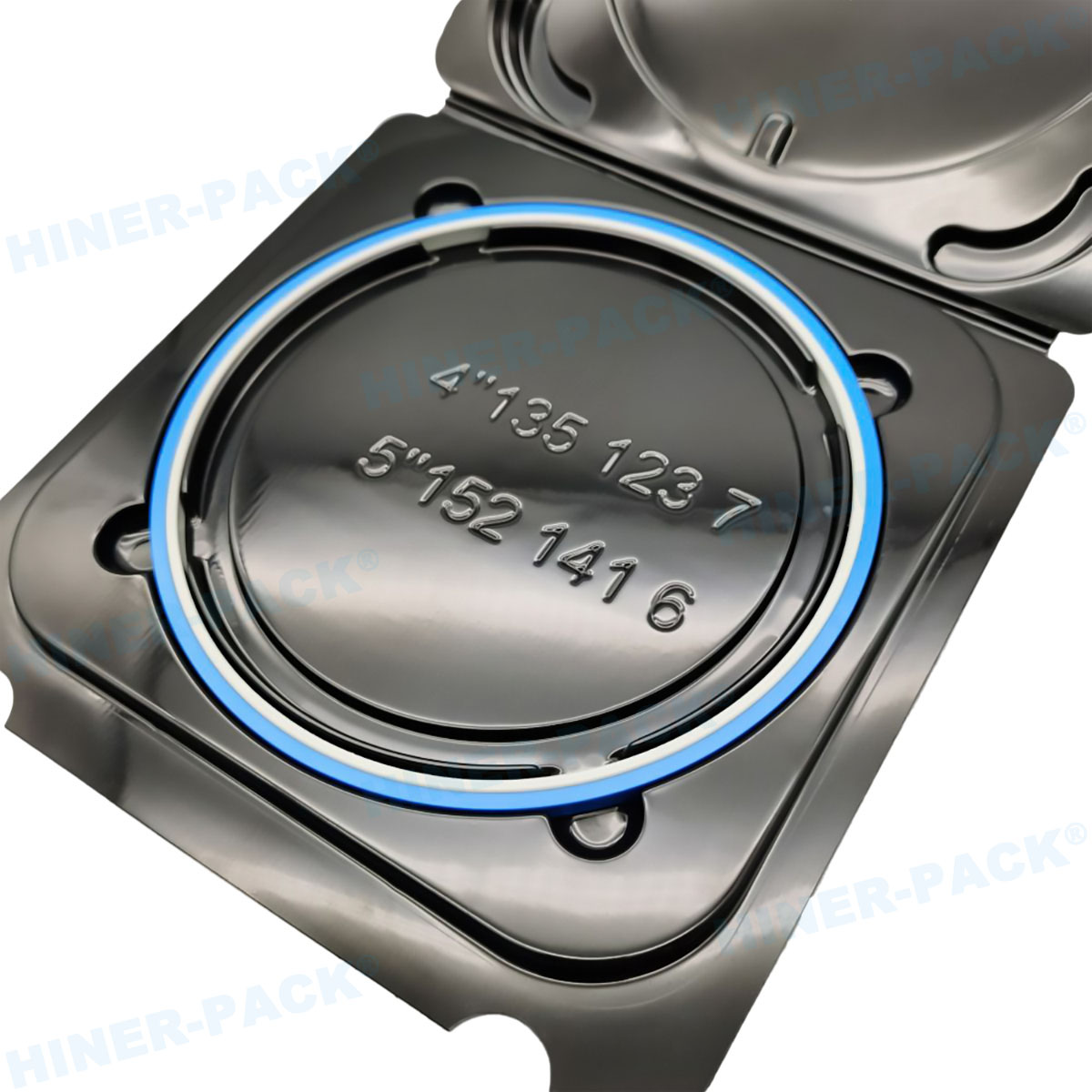
Kinematic Coupling: This is the standardized method for precisely locating the FOUP on a load port and the wafer inside the FOUP. Any wear or contamination in these couplings directly translates to placement error.
Advanced Metrology: High-resolution sensors are embedded within wafer handling robots to constantly calibrate and correct for positional drift, ensuring the end effector always knows the wafer's exact location in 3D space.
Challenge 5: Managing Electrostatic Discharge (ESD)
Static charge buildup is inevitable when non-conductive materials like silicon (which is a semiconductor but can act as an insulator) move against other surfaces. An ESD event can instantly destroy sensitive transistors.
Ionization: Strategic placement of air ionizers neutralizes static charge on wafers and wafer handling equipment.
Conductive and Static-Dissipative Materials: Using materials with controlled electrical resistance in FOUPs, end effectors, and work surfaces allows charges to bleed off safely rather than accumulating and discharging catastrophically.
Challenge 6: Integrating with the AMHS and Factory Automation
A wafer visits hundreds of tools during its manufacturing cycle. The Automated Material Handling System (AMHS)—comprising overhead hoists, rail-guided vehicles, and stockers—is the fab's circulatory system. The wafer handling system at each tool must integrate seamlessly with the AMHS.
Standardized Communication: Using protocols like SECS/GEM, the tool's wafer handling controller must communicate with the host system to receive commands, report status, and ensure the right wafer is delivered to the right tool at the right time. Any delay or miscommunication here creates a bottleneck in the entire production line.
Challenge 7: The High Cost of Ownership and Downtime
Semiconductor wafer handling equipment is capital-intensive. Beyond the initial purchase price, the Total Cost of Ownership (TCO) includes maintenance, consumables (like end effectors), and, most critically, the cost of unscheduled downtime.
Reliability Engineering: Wafer handling robots are designed for millions of cycles without failure. Predictive maintenance, using sensors to monitor motor torque and vibration, is key to preventing unexpected breakdowns.
Ease of Service: Modular designs that allow for quick replacement of high-wear components like bearings or sensors are essential for minimizing Mean Time To Repair (MTTR).
Choosing the Right Wafer Handling Solutions: A Guideline
Selecting wafer handling components is not a one-size-fits-all process. Key considerations include:
Wafer Size and Thickness: 200mm, 300mm, or emerging sizes? Are you handling thick, rigid wafers or ultra-thin, flexible ones?
Process Environment: Is it an ambient, controlled environment, or a vacuum/ultra-high vacuum chamber? Vacuum wafer handling presents unique challenges in lubrication, heat dissipation, and material outgassing.
Throughput Requirements: How many wafers per hour must the system move? This dictates the speed and acceleration requirements of the robot.
Cleanliness Class: What is the maximum allowable particulate count? This determines the material and design choices for the wafer handling system.
The Future of Semiconductor Wafer Handling
The future will be defined by "smarter" handling. We are moving towards systems equipped with more sensors (vision systems, force sensors) and AI-driven software. These systems will not just move wafers blindly; they will sense their state—checking for bowing, verifying presence, detecting edge defects on-the-fly—and make real-time decisions to optimize the process and prevent errors before they happen. The role of advanced semiconductor wafer handling will only grow more integral as the physical limits of manufacturing are pushed further.
Frequently Asked Questions (FAQs) on Semiconductor Wafer Handling
Q1: What is the single biggest cause of yield loss related to wafer handling?
A1: While mechanical damage is a serious concern, particulate contamination remains the single largest yield detractor in semiconductor wafer handling. A single microscopic particle landing on a critical area of the wafer during a process step like lithography or deposition can create a fatal defect, killing the die it lands on or even the entire wafer. This is why the core philosophy of wafer handling system design is centered on minimizing particle generation and migration.
Q2: Why are robots used almost exclusively for wafer handling instead of humans?
A2: Humans are the largest source of contamination in a cleanroom. We shed skin cells, hair, and other particles constantly. Furthermore, manual wafer handling is impossible to perform with the sub-micron precision and repeatability required for modern 300mm and larger wafers. Robots provide a sterile, highly precise, and reliable method for transporting valuable wafers, ensuring both yield and throughput goals are met.
Q3: What is a FOUP and why is it so important?
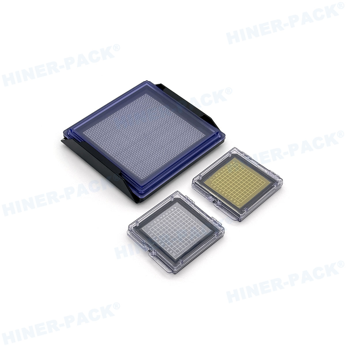
A3: A FOUP, or Front-Opening Unified Pod, is the standardized sealed container used to transport and store 300mm wafers. Its importance cannot be overstated. The FOUP is not just a box; it is a mini-cleanroom that protects the wafers from contamination, physical damage, and ESD during transit between tools in the AMHS. Its standardized design, with precise kinematic couplings, ensures it can interface correctly with any tool from any manufacturer, enabling fab-wide automation.
Q4: How does vacuum wafer handling differ from atmospheric handling?
A4: Vacuum wafer handling, used in processes like CVD and etch, is significantly more challenging. In a vacuum, there is no air, which eliminates the use of standard Bernoulli grippers and complicates heat dissipation from robot motors. Lubricants can outgas, contaminating the process chamber. Vacuum-compatible wafer handling systems often use special dry lubricants, magnetic direct-drive motors, and are constructed from materials that can withstand bake-out temperatures to remove moisture and contaminants.
Q5: What is the role of the end effector in minimizing wafer damage?
A5: The end effector is the point of physical (or near-physical) contact with the wafer and is therefore critical. Its design directly impacts the risk of mechanical and particulate damage. Key features include: being made from low-particulate, certified materials; a shape that carefully contacts only the wafer's very edge exclusion zone (a non-active area); and a surface finish that is smooth enough to prevent micro-scratches. For thin wafers, the end effector may be designed to provide broad, uniform support to prevent bending.


