
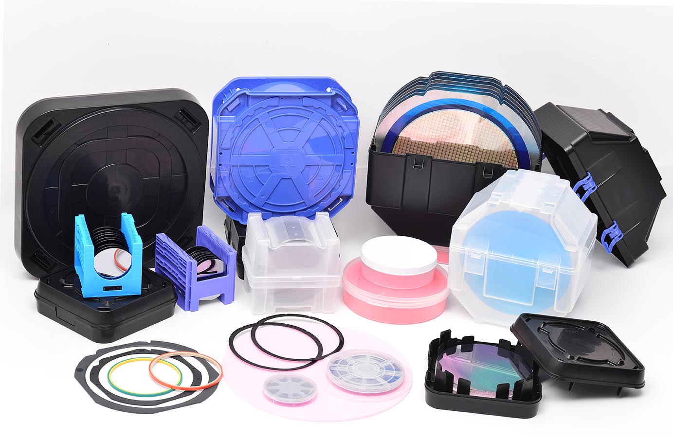
The migration to 300mm wafers and the adoption of new materials such as silicon carbide (SiC) and gallium nitride (GaN) have intensified the requirements for contamination control and electrostatic discharge (ESD) protection. In semiconductor fabrication facilities (fabs) and back-end assembly sites, the handling and transportation of wafers between process steps represent a significant risk window. ESD-safe wafer canisters are the primary line of defense against electrostatic damage, tribocharging, and airborne molecular contamination (AMC). This article dissects the engineering principles, application scenarios, and validation protocols that define modern wafer canisters, offering a decision-making framework for process and integration engineers.
1. The Physics of Failure: Quantifying ESD Risks in Wafer Transport
Electrostatic discharge remains one of the most persistent threats to yield in semiconductor manufacturing. Industry data from the ESD Association indicates that ESD-related damages account for approximately 16-22% of all field failures in microelectronic devices. In the context of bare wafers and in-process substrates, the damage is often latent—a weakened gate oxide or a metal layer degradation that escapes immediate electrical testing but leads to premature failure in the field.
When a standard polymer carrier moves through an automated material handling system (AMHS) or is subjected to vibration during shipping, triboelectric charging occurs. Voltages as low as 30-50 Volts can damage sensitive 5nm node gate oxides. ESD-safe wafer canisters mitigate this by incorporating materials with surface resistivity typically in the range of 105 to 1011 Ohms/square, allowing charges to dissipate slowly and evenly without generating a damaging spark. The key parameter is the charge decay time (less than 2 seconds per MIL-STD-3010 or ESD STM11.11), ensuring any accumulated charge is neutralized before the wafer is removed.
2. Material Science and Structural Integrity
2.1 Conductive vs. Dissipative Polymers
The selection of polymer matrix and filler is critical. While carbon-fiber or carbon-powder filled polycarbonate (PC) or polyetheretherketone (PEEK) are common, the dispersion uniformity dictates performance. Inhomogeneous filler distribution can create localized conductive "hot spots" that might act as charge collectors. Modern ESD-safe wafer canisters often utilize inherently dissipative polymers (IDPs) or precise compounding of additives to achieve stable resistivity across the entire temperature and humidity range (-40°C to 125°C) required by supply chain logistics.
2.2 Outgassing and Cleanroom Compatibility
Outgassing (measured via ASTM E595) must be minimized to prevent condensation on wafer surfaces. Total Mass Loss (TML) should be below 1.0% and Collected Volatile Condensable Material (CVCM) below 0.1%. Hiner-pack, a specialist in polymer wafer handling solutions, ensures that its Hiner-pack canisters meet or exceed these thresholds, making them suitable for ISO Class 3 or cleaner environments. The structural ribs and gate design also influence particle generation; smooth, radiused surfaces prevent abrasion and particle shedding during automated pick-and-place.
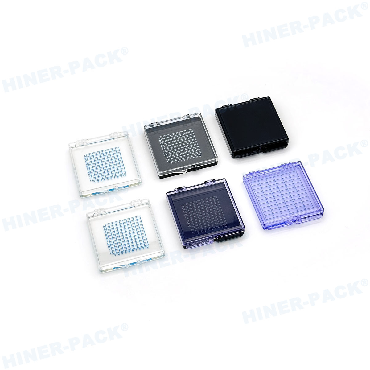
3. Design Specifications: Interoperability with 200mm and 300mm Standards
Wafer canisters are not one-size-fits-all. They must interface with FOUPs (Front Opening Unified Pods), FOSBs (Front Opening Shipping Boxes), and process equipment load ports. Critical design elements include:
Wafer pitch and capacity: Standard configurations hold 13 or 25 wafers, with precise slot-to-slot spacing (e.g., 10mm for 300mm) to prevent cross-slot contact.
Kinematic coupling interfaces: Ensures repeatable alignment on load ports, critical for automated handling.
RFID or barcode integration: Enables traceability within the MES (Manufacturing Execution System).
Sealing and gasket design: Dual o-ring seals or labyrinth seals protect against pressure differentials and moisture ingress during air transport.
Engineers should verify that the chosen ESD-safe wafer canisters comply with SEMI standards (such as SEMI E47 for FOUBs and SEMI M31 for wafer shippers) to ensure seamless integration into existing 300mm fab infrastructures.
4. Application-Specific Performance Criteria
4.1 Front-End-of-Line (FEOL) Sensitive Layers
After gate oxidation or ion implantation, wafers are extremely sensitive to charge. Here, canisters must provide Faraday cage-like protection. This requires conductive materials that can be grounded through the load port. Tests using a charged plate monitor (CPM) inside a canister during simulated AMHS transport should show induced voltages below 10V.
4.2 Back-End-of-Line (BEOL) and Thin-Wafer Handling
Thinned wafers (below 100µm) for 3D stacking and advanced packaging are mechanically fragile. Canisters designed for these applications incorporate low-friction wafer supports and gentle retention mechanisms. The internal surface roughness and material hardness are optimized to prevent edge chipping.
4.3 Inter-facility Shipping
For wafers shipped between fabs or to OSAT (Outsourced Semiconductor Assembly and Test) facilities, canisters must withstand vibration, shock, and atmospheric changes. Vacuum-sealed or nitrogen-purge capable canisters, often referred to as "shippers," are essential. Hiner-pack offers customized solutions that integrate pressure equalization valves while maintaining ESD safety, preventing "wafer popping" due to rapid pressure changes during flight.
5. The Cost of Non-Compliance: Yield Impact and Field Failures
A semiconductor manufacturer might save a few dollars per unit by using generic carriers. However, the total cost of ownership (TCO) analysis tells a different story. A single ESD event can ruin an entire lot of 25 wafers, representing hundreds of thousands of dollars in lost value. Furthermore, latent ESD damage in customer hands leads to RMA (Return Material Authorization) costs and brand reputation damage. Investing in qualified ESD-safe wafer canisters from reputable suppliers like Hiner-pack is a risk mitigation strategy validated by reliability engineers. Independent testing by third-party labs (e.g., electrostatic decay per FTMS-101C) should be requested as part of the qualification process.
6. Validation Protocols and Incoming Quality Control (IQC)
To ensure that your ESD-safe wafer canisters perform as specified, a robust qualification procedure is necessary. Key tests include:
Surface resistivity mapping: Measure at multiple points (inside slots, outer walls) per ASTM D257.
Charge decay time: Using a charged plate method, verify dissipation from ±1000V to ±10V in <2 seconds.
Particle contribution test: Agitate the canister in a cleanroom environment and measure particles >0.1µm with a liquid particle counter (LPC).
Extractable metals and anions: Ion chromatography to detect potential ionic contamination (Cl-, Na+, K+).
Mechanical shock and vibration: Simulated transport profiles (ISTA 3A) to ensure wafer integrity.
7. Future Trends: Automation and Industry 4.0 Integration
As fabs move towards fully autonomous 300mm and emerging 450mm pilot lines, wafer canisters become "smart" assets. Embedded sensors for humidity, shock, and tamper detection are being integrated. ESD-safe materials must now also be compatible with wireless data transmission without interfering with signals. Hiner-pack is actively developing next-generation canisters that combine ESD-safe properties with RFID sensor platforms, enabling real-time tracking of wafer environmental history. The convergence of ESD protection and digital traceability will define the next decade of wafer logistics.
Frequently Asked Questions (FAQ)
Q1: What is the difference between a "conductive" and a "dissipative"
ESD-safe wafer canister?
A1: The distinction is based on surface
resistivity. Conductive materials have a surface resistivity less than
105 Ohms/square and can discharge quickly, but may cause rapid
current flow that could damage extremely sensitive devices. Dissipative
materials range from 105 to 1011 Ohms/square and allow a
slower, controlled dissipation of charge. Most wafer canisters used in sensitive
processes are dissipative to avoid high discharge currents.
Q2: Can ESD-safe wafer canisters be cleaned and reused, and if so,
what is the recommended method?
A2: Yes, high-quality canisters made
from polycarbonate or PEEK are designed for multiple uses. The recommended
cleaning procedure typically involves deionized (DI) water with a mild
surfactant, followed by rinsing and drying in a Class 100 environment.
Aggressive solvents or ultrasonic cleaning can degrade the ESD properties over
time and should be validated with the supplier, such as Hiner-pack, for compatibility.
Q3: How do I verify that a used canister is still
ESD-safe?
A3: Regular auditing with a surface resistance meter
(concentric ring probe) according to ANSI/ESD S11.11 is recommended.
Measurements should be taken on the wafer contact surfaces (the slots) and the
external handling surfaces. A significant drift out of the specified range
(e.g., >1011 Ohms) indicates that the ESD additive has worn out or
been contaminated.
Q4: Are ESD-safe wafer canisters required for 200mm wafers, or only
for 300mm?
A4: Absolutely required for all wafer sizes. While 300mm
fabs have standardized on FOUPs with ESD control, 200mm operations still rely
heavily on wafer canisters and shippers. As device nodes shrink even on 200mm
wafers (e.g., power semiconductors, MEMS), the sensitivity to ESD increases.
Proper ESD-safe wafer canisters are a universal requirement regardless of form factor.
Q5: What role do these canisters play in preventing "soft failures"
like data retention loss in memory devices?
A5: A significant role.
Soft failures are often caused by low-level ESD events that partially degrade a
memory cell or logic gate. The canister prevents the triboelectric charging that
occurs when wafers rub against non-ESD materials during transport. By
maintaining a low-static environment, the risk of latent damage is minimized,
thereby improving long-term reliability parameters such as data retention in
NAND or DRAM.
Q6: Can I use the same ESD-safe wafer canisters for both bare silicon
wafers and epitaxial wafers?
A6: Yes, generally the same canisters
are suitable, provided they are clean and free of contaminants. However, for
epi-wafers with specific surface chemistries, it is crucial to ensure that the
outgassing profile of the canister does not introduce dopants or contaminants
that could affect the epitaxial layer. Consultation with the canister
manufacturer regarding material composition is advised.
Selecting the appropriate ESD-safe wafer canisters is a multi-faceted engineering decision that impacts yield, reliability, and operational efficiency. From material resistivity and cleanroom compatibility to automated handling standards, each parameter must be scrutinized. Suppliers like Hiner-pack combine deep polymer science knowledge with semiconductor industry standards to deliver solutions that protect the wafer throughout its journey. As device geometries continue to shrink and new materials are introduced, the role of advanced wafer canisters as a critical control point will only grow in importance.


