When you are dealing with silicon wafers worth thousands of dollars, the last thing you want to worry about is the box they travel in. Yet, shipping damage remains a leading cause of yield loss in the semiconductor supply chain. The humble container—often just an afterthought in the fabrication process—is actually the first line of defense against the chaotic world of logistics.
This brings us to the importance of the wafer pack. Whether you are shipping raw silicon slices, finished pattern wafers, or delicate glass substrates, the container determines if your product arrives ready for lithography or ready for the scrap bin. Companies like Hiner-pack have spent years refining these designs because they understand that in this industry, there is no margin for error.
This article skips the generic advice and looks at the engineering realities of selecting the right packaging for international semiconductor transport.
What is a Wafer Pack and Why Does it Matter?
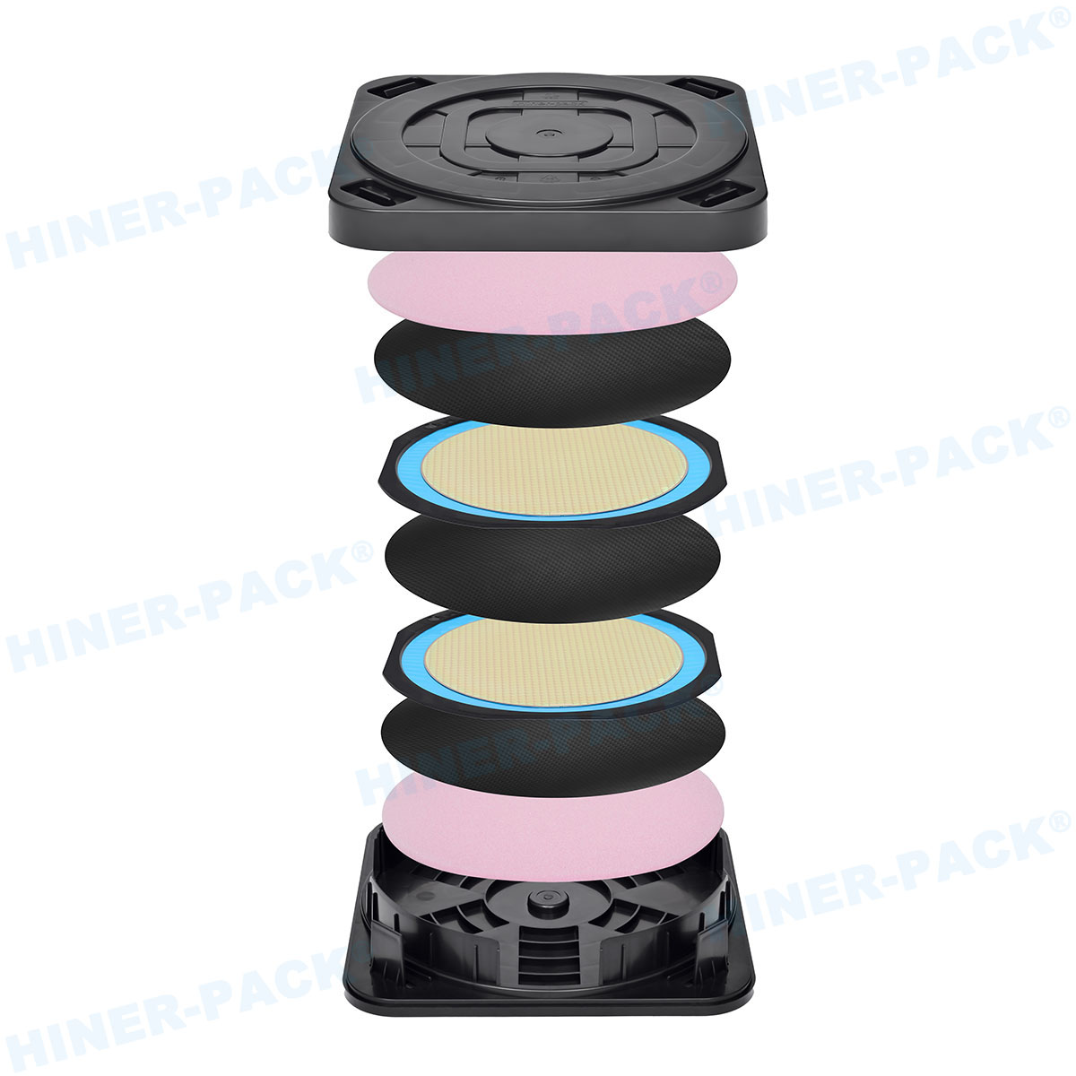
A wafer pack is not simply a plastic tub. It is an engineered isolation chamber designed to protect semiconductor wafers from three specific enemies: physical shock, electrostatic discharge (ESD), and particulate contamination.
In the international semiconductor field, these packs come in various configurations. You might see them referred to as coin shippers, jars, canisters, or cassettes. Regardless of the name, the function remains the same. They must immobilize the wafer so it does not rattle, yet hold it gently enough to prevent stress fractures.
If you choose the wrong specifications, you risk "wafer haze"—a condition where outgassing from cheap plastic condenses on the wafer surface. This renders the silicon unusable for high-precision applications.
Material Selection for Your Wafer Pack
The plastic used in your container dictates its performance. You cannot simply use generic polymer and expect it to work in a Class 100 cleanroom.
Polypropylene (PP) is the standard workhorse. It is durable, naturally low in outgassing, and cost-effective. For most standard shipping needs, a wafer pack made from high-purity PP is sufficient.
However, for sensitive electronics, you need ESD-safe materials. Standard plastics generate static electricity when rubbed. If a wafer slides slightly inside a jar during a flight, that static builds up. When a technician opens the jar, zap—the circuit is fried. Carbon powder or carbon fibers are often added to the plastic matrix to create a conductive or static-dissipative path, grounding the charge safely.
For high-temperature or chemical-resistant applications, materials like PFA (Perfluoroalkoxy) or PEEK are used, though these drive up the cost significantly.
The Role of the Wafer Pack in Preventing Micro-Cracks
Vibration is unavoidable. Trucks hit potholes; planes experience turbulence. A poorly designed wafer pack transfers that energy directly to the brittle silicon.
The design must incorporate suspension. In "coin style" shippers, this is often achieved through a spider-spring mechanism in the lid and base. These plastic springs compress when the pack is closed, holding the wafer edges firmly.
If the tension is too loose, the wafer rotates. This rotation acts like a grinder, creating microscopic silicon dust. This dust then migrates to the active area of the die, causing short circuits. If the tension is too tight, the center of the wafer creates a pressure point, leading to micro-cracks that might not be visible until the wafer undergoes thermal stress later in manufacturing.
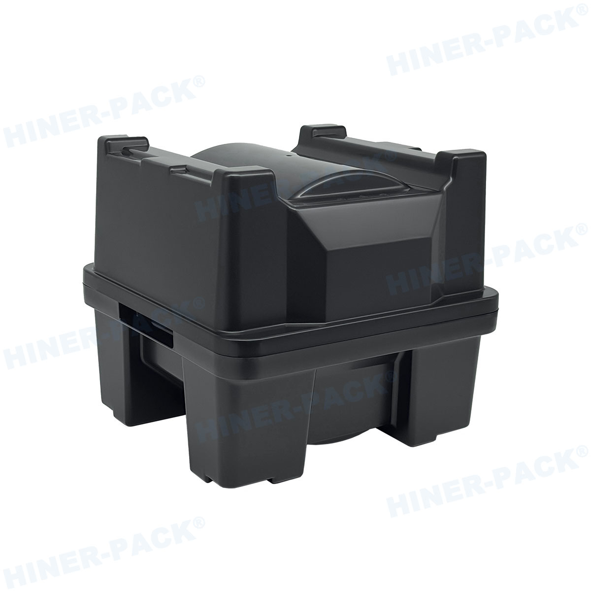
Single Shippers vs. Multi-Wafer Canisters
The choice between shipping wafers individually or in bulk depends on your specific stage in the supply chain.
Single wafer shippers are the standard for high-value, finished wafers or reticles. If one pack is crushed by a forklift, you only lose one unit. They are also easier to inspect upon receipt without exposing a whole batch to the air.
Multi-wafer canisters (often holding 25 wafers) are the standard for raw silicon production. They are efficient and dense. However, the engineering challenge here is the slot pitch. The wafer pack must ensure that wafers do not touch each other, even when the box is dropped. This requires high-precision injection molding to ensure the internal slots are perfectly parallel.
Cleanliness Standards in Wafer Packaging
A wafer pack must be clean before it ever touches a wafer. This seems obvious, but the definition of "clean" varies.
Manufacturers wash these containers in industrial lines using deionized water and surfactants, followed by vacuum drying. They are then double-bagged in a cleanroom environment.
When sourcing your packaging, you must ask about the particle count validation. Are they certified for ISO Class 4 or Class 5? Hiner-pack has focused heavily on this aspect, ensuring that their packaging lines meet strict particulate standards so that the box doesn't become the source of contamination.
The Impact of Automation on Pack Design
Modern fabs are removing humans from the loop. This means the wafer pack is often handled by a robot, not a hand.
The physical dimensions must be exact. If the flange on a cassette is off by a millimeter, the robotic end-effector might drop the load. Or worse, the robot might crush the cassette trying to grip it.
Dimensional stability over time is key here. Cheap plastics can warp after repeated washing cycles or exposure to heat. A warped cassette jams the load port, causing downtime that costs thousands of dollars per minute.
Sustainability and Reusability in the Supply Chain
The semiconductor industry generates massive amounts of plastic waste. There is a growing push to reuse shipping containers.
A single-use wafer pack is wasteful, but a reusable one requires a reverse logistics chain. The pack must be robust enough to survive the round trip, the washing process, and the return shipment.
Durability becomes the primary purchasing factor here. Hinges and latches are usually the first failure points. Living hinges (where the plastic just bends) eventually fatigue and snap. Pin-hinges are more durable but harder to clean. Balancing these factors is vital for a green supply chain.
Innovation at Hiner-pack
It is worth noting how specific brands are tackling these issues. Hiner-pack has carved out a niche by focusing on the balance between cost and high-performance protection.
Rather than just copying standard designs, they have looked at the common pain points—specifically latch failure and particle generation. By refining the mold flow analysis during production, they produce containers with lower internal stress. This means the plastic is less likely to warp over time, ensuring a secure seal for more trips.
Cost Considerations and ROI
Procurement teams often look at the unit price of a wafer pack. This is a mistake. The real cost is the "cost of ownership."
If a cheap pack has a 1% higher failure rate, the loss of silicon far outweighs the savings on the plastic. Furthermore, if the pack cannot be reused, you are constantly buying new stock.
High-quality packs might cost 30% more upfront but can last for 50 cycles instead of 10. The math heavily favors investing in quality engineering.
Final Thoughts on Wafer Logistics
The journey of a semiconductor is long and hazardous. From the crystal puller to the final assembly house, the silicon travels thousands of miles. The only thing protecting that investment is the plastic shell around it.
Don't let the packaging be the weak link in your chain. Whether you are using a standard generic container or a specialized solution from Hiner-pack, ensure you understand the material properties, the mechanical design, and the cleanliness standards.
Your yield depends on it.
Frequently Asked Questions (FAQ)
Q1: What is the best material for a wafer pack to prevent static damage?
A1: The best material for preventing static damage is usually Polypropylene (PP) or Polycarbonate (PC) blended with carbon powder or carbon fiber. This creates a conductive or static-dissipative material that safely grounds any electrical charge, preventing ESD events that could destroy sensitive wafer circuits.
Q2: Can I reuse a single-wafer shipper?
A2: Yes, most single-wafer shippers are designed to be reusable. However, they must undergo a rigorous cleaning process between uses. You must inspect the container for scratches, loose particles, or damaged springs before reusing it. If the internal retention springs are fatigued, the pack should be discarded.
Q3: How do I choose the right size wafer pack?
A3: You must match the pack exactly to the diameter of your wafer (e.g., 2-inch, 4-inch, 150mm, 200mm, 300mm). Using a pack that is slightly too large will allow the wafer to rattle and break. Additionally, consider the thickness of your wafers; some packs are designed for standard thickness (approx. 500-700 microns), while thinner wafers require specialized spacers.
Q4: What causes "wafer haze" inside a pack?
A4: Wafer haze is often caused by outgassing. This happens when the plastic of the wafer pack releases volatile organic compounds (VOCs) or moisture over time. These molecules condense on the silicon surface. To prevent this, use high-purity, low-outgassing materials and ensure the packs are stored in a temperature-controlled environment.
Q5: What is the difference between a cassette and a coin shipper?
A5: A coin shipper is a horizontal container usually designed for a single wafer (sometimes a small stack with spacers), offering maximum protection for individual high-value units. A cassette is a vertical slotted rack designed to hold multiple wafers (usually 25) spaced apart. Cassettes are typically used for mass processing and bulk shipping.


