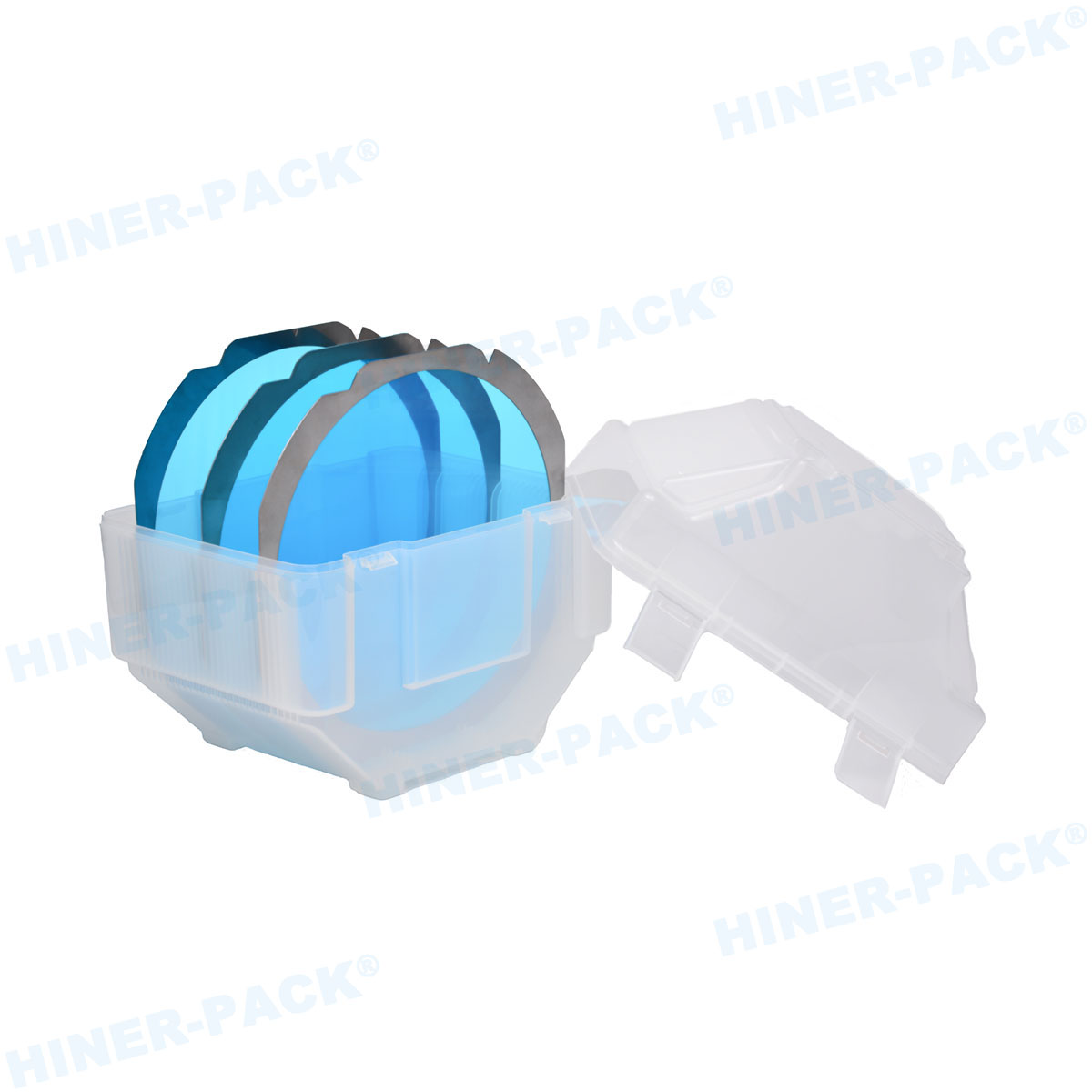
In the highly precise world of semiconductor manufacturing, where a single particle of dust can spell disaster for a batch of chips worth millions, the humble semiconductor wafer box plays an outsize role. Often overlooked, these containers are the primary guardians of silicon wafers as they travel between fabrication, testing, and assembly. Choosing the wrong box isn't just an inconvenience; it's a direct threat to yield, profitability, and product reliability. This guide breaks down the seven most critical factors you must consider when selecting semiconductor wafer boxes for your operation, helping you make an informed decision that protects your most valuable assets.
1. Material Matters: Beyond Basic Plastics
Not all plastics are created equal, especially in a cleanroom environment. The material of your wafer shipping boxes must meet stringent requirements.
PFA (Perfluoroalkoxy): The gold standard for high-purity applications. PFA offers excellent chemical resistance, minimal particle shedding, and can withstand repeated high-temperature sterilization, making it ideal for front-end processes.
PPS (Polyphenylene Sulfide): Known for its exceptional dimensional stability and resistance to high temperatures, PPS is a robust choice for demanding thermal processes.
PC (Polycarbonate) & PP (Polypropylene): Often used for less critical stages or in wafer cassette storage. While cost-effective, they may not offer the same level of purity or temperature resistance as PFA or PPS.
Leading suppliers like Hiner-pack specialize in crafting boxes from these high-performance polymers, ensuring material consistency and traceability.
2. The Purity Imperative: Minimizing Contamination
Contamination is the enemy. The primary function of a wafer storage container is to be cleaner than the environment it's protecting.
Outgassing: Low outgassing materials are essential to prevent airborne molecular contaminants (AMCs) from depositing on wafer surfaces.
Static Control: Dissipative or conductive materials are often required to prevent electrostatic discharge (ESD), which can attract particles and damage delicate circuit features.
Surface Smoothness: A flawlessly smooth interior surface minimizes the risk of particles adhering to the box and subsequently transferring to the wafers.
3. Mechanical Integrity: Protecting Against Physical Damage
Wafers are incredibly fragile. A wafer handling box must provide superior mechanical protection.
Impact Resistance: The box must withstand the bumps and jolts of automated material handling systems (AMHS) and manual transport without cracking or compromising its seal.
Durability: Look for boxes designed for hundreds of cycles. Cheap, single-use alternatives create waste and can be more expensive in the long run. Hiner-pack's designs, for instance, are rigorously tested for cycle life, ensuring they remain reliable over time.
Stackability: Secure and stable stacking is crucial for efficient floor space utilization in cleanrooms and storage areas.
4. Compatibility: Ensuring a Seamless Fit
Your new semiconductor wafer boxes cannot exist in a vacuum. They must integrate perfectly with your existing infrastructure.
Automation Compatibility: The box must have the correct dimensions, notch locations, and robotic handling features to interface flawlessly with your AMHS, load ports, and processing tools.
Cassette Compatibility: Ensure the box is designed to hold the standard or custom wafer cassettes (FOUPs, FOSBs, etc.) you use.
Sealing Technology: The integrity of the seal is paramount. Whether it's a passive seal for clean storage or a sophisticated filter system for mini-environment control in FOUPs, the seal must be reliable and consistent.
5. Capacity and Wafer Size: Planning for the Future
The industry's march towards larger wafers continues.
Common Sizes: While 200mm and 300mm wafers are current workhorses, production of 450mm, though slowed, remains a future consideration for some.
Capacity: Boxes are designed to hold a specific number of wafers (e.g., 25-wafer capacity is common). Selecting the right capacity balances transport efficiency with the risk of damage from over-crowding.
Forward Compatibility: Investing in a modular system that can adapt to future wafer size changes can provide significant long-term savings.
6. Traceability and Identification
In an industry governed by strict quality control, knowing the history of every component is non-negotiable.
RFID Tags: Modern wafer shipping boxes often come with embedded RFID tags that store a unique identifier. This allows for seamless tracking through the entire manufacturing lifecycle.
Barcode Labels: A more traditional but still effective method for identification.
Data Matrix Codes: Direct part marking (DPM) with Data Matrix codes on the box itself provides a permanent and reliable identification method.
7. Total Cost of Ownership (TCO) Over Sticker Price
The cheapest box off the shelf is rarely the most economical.
Initial Purchase Price: This is just the starting point.
Cycle Life: A box that costs twice as much but lasts five times longer offers a much lower cost-per-cycle.
Cleaning and Maintenance: Consider the cost and frequency of required cleaning to maintain purity standards. High-quality boxes from suppliers like Hiner-pack are often designed for easy, effective cleaning.
Yield Impact: This is the most significant factor. A single box-related contamination event that causes a lot to be scrapped can wipe out years of savings from buying inferior containers. Investing in reliable semiconductor wafer boxes is, fundamentally, an investment in yield protection.
Frequently Asked Questions (FAQs)
Q1: How often should semiconductor wafer boxes be cleaned and inspected?
A1: The cleaning and inspection frequency depends entirely on the process step and the cleanroom class. For highly sensitive front-end processes, boxes may be cleaned after every single use. A standard practice in many fabs is a regular cleaning schedule—after 5 to 10 cycles—accompanied by a rigorous inspection for physical damage, surface wear, and seal integrity. Always follow your facility's strict contamination control protocol.
Q2: Can we use generic wafer boxes to save costs?
A2: While generic or off-spec wafer storage containers may have a lower upfront cost, they pose a significant risk. They often lack the certified low outgassing, consistent ESD properties, and robotic handling precision of branded boxes from trusted suppliers like Hiner-pack. The potential cost of yield loss due to contamination or misprocessing far outweighs the initial savings.
Q3: What is the difference between a FOUP and a standard wafer box?
A3: A FOUP (Front-Opening Unified Pod) is a specific type of wafer handling box designed for 300mm wafers. Its key differentiator is that it features a built-in mini-environment with a nitrogen purge and filtration system, allowing it to interface directly with process tools without exposing the wafers to the cleanroom air. A standard wafer box is typically a more passive container for transport or storage.
Q4: Are there environmentally friendly options for wafer boxes?
A4: Yes, the industry is moving towards sustainability. The most significant green practice is selecting durable, long-lasting boxes designed for hundreds of cycles, thereby reducing plastic waste. Some manufacturers, including Hiner-pack, also offer recycling programs for their semiconductor wafer boxes at end-of-life, and explore the use of high-performance recyclable polymers where technically feasible.
Q5: How do I properly dispose of or recycle old wafer boxes?
A5: You should never dispose of semiconductor wafer boxes as regular plastic waste. Due to potential chemical contamination, they require special handling. The best practice is to contact your supplier. Many, like Hiner-pack, have established take-back or recycling programs to ensure the materials are processed responsibly and in compliance with environmental regulations, preventing hazardous materials from entering landfills.


