In the fast-paced world of semiconductor manufacturing, the safe and efficient transport of wafers is a critical yet often overlooked aspect. Semiconductor wafer shipping involves the logistics of moving fragile, high-value silicon wafers from fabrication facilities to assembly plants or clients worldwide. Any mishandling during transit can lead to catastrophic losses, including wafer breakage, contamination, or electrostatic discharge damage, potentially costing millions in revenue. As the demand for smaller, more powerful chips grows, so does the complexity of wafer logistics. Companies like Hiner-pack have emerged as key players, offering specialized packaging and shipping solutions tailored to the semiconductor industry's stringent requirements. This article delves into the practical aspects of semiconductor wafer shipping, covering solutions, customization options, manufacturer insights, pricing factors, and best practices to help businesses optimize their supply chains.
The Critical Role of Semiconductor Wafer Shipping in the Global Supply Chain
Semiconductor wafer shipping is not just about moving products from point A to point B; it's about ensuring that these delicate components arrive intact and uncontaminated. Wafers, typically made of silicon and ranging from 150mm to 450mm in diameter, are the foundation of electronic devices. They are extremely sensitive to physical shock, temperature fluctuations, humidity, and electrostatic discharge. A single damaged wafer can disrupt production lines, delay product launches, and result in significant financial losses. In recent years, the globalization of semiconductor manufacturing has intensified the need for reliable shipping methods. For instance, wafers produced in Asia might be shipped to testing facilities in Europe or the Americas, requiring robust logistics frameworks. Companies like Hiner-pack have developed advanced packaging systems that address these challenges, incorporating materials that shield wafers from environmental hazards. By focusing on semiconductor wafer shipping, businesses can minimize risks and maintain the integrity of their products throughout the supply chain.
Common Challenges in Semiconductor Wafer Shipping and How to Overcome Them
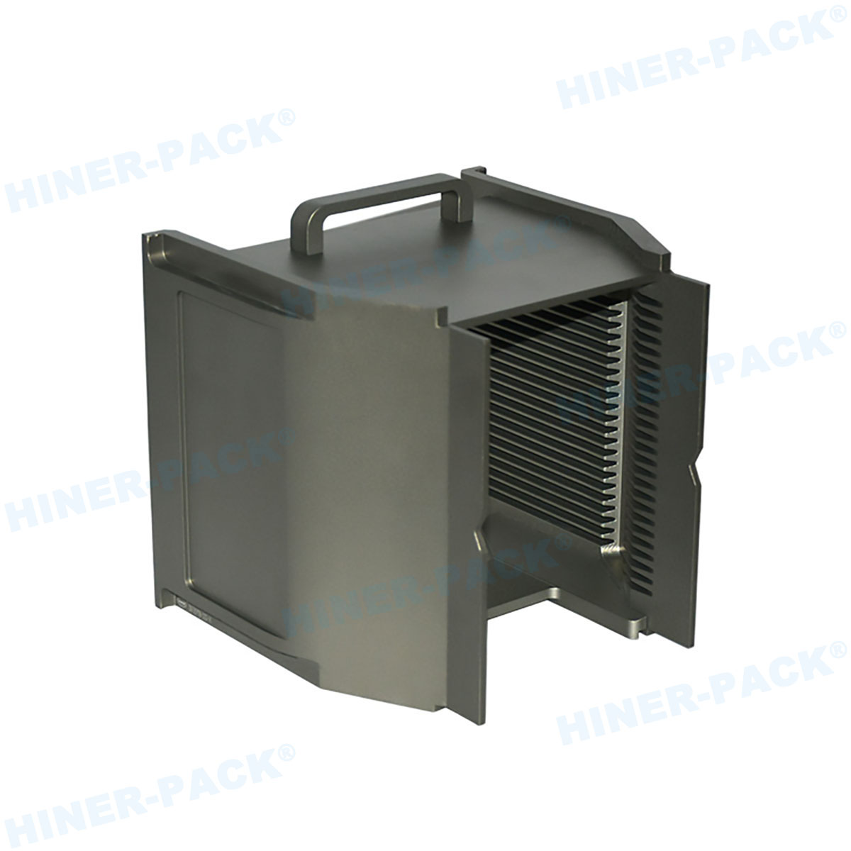
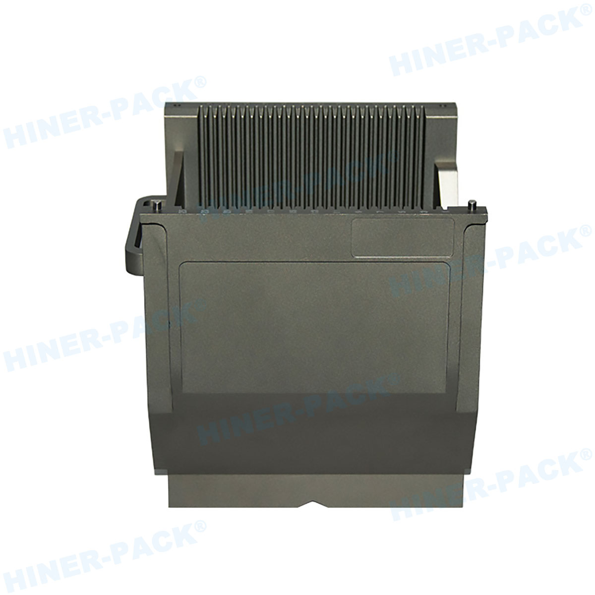
The process of semiconductor wafer shipping presents several hurdles that manufacturers and logistics providers must navigate. One major issue is physical damage due to vibration or impact during transit. Wafers are brittle and can crack if not properly cushioned. Another challenge is contamination from particles, moisture, or chemicals, which can render wafers unusable. Additionally, electrostatic discharge (ESD) poses a silent threat, as it can damage the intricate circuits on wafers without visible signs. To mitigate these risks, industry leaders have adopted specialized solutions. For example, using ESD-safe containers made from conductive materials can prevent static buildup. Temperature-controlled shipping environments help maintain wafer integrity, especially for sensitive materials like gallium arsenide. Hiner-pack, among others, offers customized packaging that includes vacuum-sealed trays and shock-absorbent designs. By partnering with experienced providers, companies can implement proactive measures, such as real-time tracking and humidity monitors, to ensure safe semiconductor wafer shipping.
Custom Solutions for Semiconductor Wafer Shipping: Tailoring to Your Needs
Every semiconductor operation has unique requirements, making customization a vital aspect of wafer shipping. Off-the-shelf solutions often fall short in addressing specific needs, such as handling oversized wafers or complying with international regulations. Custom semiconductor wafer shipping options can include bespoke packaging designs, specialized labeling for traceability, and integrated logistics services. For instance, some manufacturers require multi-layer containers that accommodate wafers of varying thicknesses, while others need anti-tamper features for high-security shipments. Hiner-pack excels in this area by offering tailored services, such as designing foam inserts that fit exact wafer dimensions or developing reusable shipping containers to reduce waste and costs. Customization also extends to documentation and compliance, ensuring that shipments meet regional standards for hazardous materials or export controls. By investing in personalized semiconductor wafer shipping strategies, companies can enhance efficiency, reduce damage rates, and build stronger supply chain resilience.
Selecting the Right Manufacturer for Semiconductor Wafer Shipping Supplies
Choosing a reliable manufacturer for shipping supplies is crucial in the semiconductor industry. The right partner should offer high-quality materials, innovation, and industry expertise. Key factors to consider include the manufacturer's track record in handling fragile components, their ability to provide ESD-protective packaging, and their compliance with international standards like SEMI or ISO. For example, manufacturers that produce wafer shippers with built-in humidity indicators or RFID tracking capabilities add significant value. Hiner-pack has built a reputation for delivering durable, cost-effective solutions, such as their range of conductive boxes and desiccant-loaded containers that protect wafers during long-haul transports. When evaluating manufacturers, it's essential to assess their customization capabilities, lead times, and after-sales support. A good manufacturer will conduct thorough testing, such as drop tests and climate simulations, to validate their products. By selecting a trusted provider for semiconductor wafer shipping needs, businesses can ensure consistent quality and minimize supply chain disruptions.
Understanding Pricing Factors in Semiconductor Wafer Shipping
Cost is a significant consideration in semiconductor wafer shipping, as budgets must balance affordability with the need for high protection. Pricing depends on various factors, including the type of packaging materials, shipping distance, volume, and additional services like insurance or expedited delivery. Standard wafer shipping boxes might cost a few dollars per unit, but custom ESD-safe containers can run higher due to specialized materials and design. For international shipments, factors like customs duties, fuel surcharges, and handling fees add to the overall expense. Companies can optimize costs by bulk ordering, negotiating contracts with logistics partners, or adopting reusable packaging systems. Hiner-pack offers competitive pricing models that scale with volume, helping firms manage expenses without compromising on safety. It's also wise to consider the total cost of ownership—inexpensive packaging that leads to damaged wafers can be far more costly in the long run. By analyzing these pricing factors, businesses can make informed decisions that align with their financial and operational goals in semiconductor wafer shipping.
Best Practices for Safe and Efficient Semiconductor Wafer Shipping
Implementing best practices in semiconductor wafer shipping can drastically reduce risks and improve overall efficiency. Start with proper packaging: use rigid, ESD-safe containers with adequate cushioning to absorb shocks. Ensure that wafers are stored in cleanroom conditions before sealing to prevent contamination. During transit, maintain a controlled environment with stable temperature and humidity levels, especially for sensitive wafers. Labeling is critical—clearly mark packages with handling instructions, such as "Fragile" or "Keep Dry," and use barcodes or RFID for real-time tracking. Training staff on proper handling procedures, including how to load and unload wafers without causing stress, is equally important. Regularly audit your shipping processes and collaborate with logistics providers to address any gaps. Hiner-pack integrates these practices into their solutions, offering training and support to clients. Additionally, document every shipment meticulously, including condition reports and insurance details, to facilitate claims if issues arise. By adhering to these best practices, companies can achieve reliable semiconductor wafer shipping that supports continuous production and customer satisfaction.
In conclusion, semiconductor wafer shipping is a cornerstone of the global electronics supply chain, demanding precision, customization, and cost-effectiveness. From addressing common challenges to selecting the right manufacturers and implementing best practices, every step plays a vital role in safeguarding these high-value components. Brands like Hiner-pack demonstrate how innovation in packaging and logistics can transform wafer transport into a seamless process. As technology evolves, staying updated on trends such as smart packaging and sustainable materials will be key. By prioritizing robust semiconductor wafer shipping strategies, businesses can not only protect their investments but also drive growth in an increasingly competitive market.
Frequently Asked Questions (FAQ)
Q1: What are the main risks associated with semiconductor wafer shipping?
A1: The primary risks include physical damage from shock or vibration, contamination from particles or moisture, and electrostatic discharge (ESD) that can harm wafer circuits. These issues can lead to costly rejections and production delays, making it essential to use specialized packaging and controlled shipping environments.
Q2: How can I reduce costs in semiconductor wafer shipping without compromising safety?
A2: To cut costs, consider bulk ordering of packaging supplies, negotiating long-term contracts with logistics providers, and opting for reusable containers. Additionally, work with manufacturers like Hiner-pack that offer scalable solutions and focus on total cost of ownership rather than just upfront prices.
Q3: What customization options are available for semiconductor wafer shipping?
A3: Customization can include tailored container sizes and shapes, integrated humidity and ESD controls, specialized labeling for tracking, and compliance features for international regulations. Providers such as Hiner-pack often design bespoke solutions based on specific wafer dimensions and transport routes.
Q4: Why is ESD protection crucial in semiconductor wafer shipping?
A4: ESD protection is vital because static electricity can irreparably damage the microscopic circuits on wafers, often without visible signs. Using ESD-safe materials in packaging, like conductive plastics or metals, prevents static buildup and ensures wafer integrity during transit.
Q5: How do I choose a reliable manufacturer for wafer shipping supplies?
A5: Look for manufacturers with a proven track record in the semiconductor industry, certifications like SEMI or ISO, and the ability to provide customized, tested solutions. Evaluate their product range, lead times, and customer support—companies like Hiner-pack often stand out due to their industry expertise and innovative offerings.


