
The transition to 12-inch semiconductor manufacturing has raised the stakes for logistics and handling. When a single cassette holds twenty-five wafers worth tens of thousands of dollars, the container itself becomes a critical component of the yield equation.
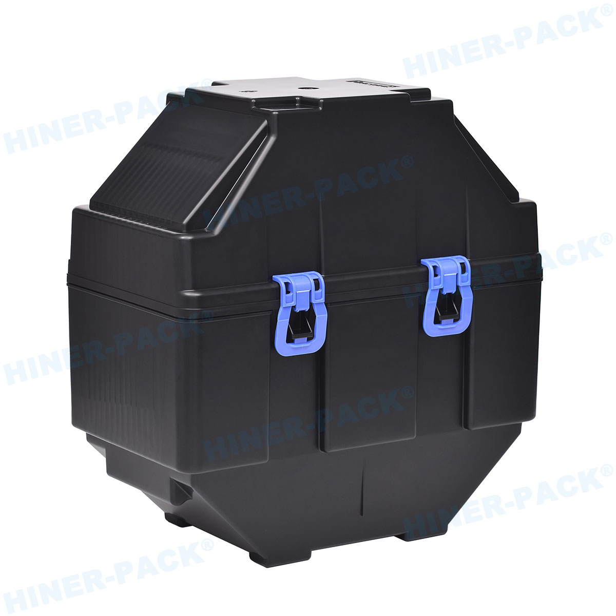
300mm wafer carriers are not merely plastic boxes; they are sophisticated micro-environments designed to isolate silicon from the chaos of the outside world. From the moment a wafer leaves the polishing pad to the final sort, it relies on these pods for protection against particles, vibration, and electrostatic discharge.
For fab managers and process engineers, selecting the right carrier system is about risk mitigation. A failure in the latch mechanism or a slight warping of the chassis can lead to automated handling errors, causing machine downtime or catastrophic wafer breakage.
At Hiner-pack, we understand that the reliability of your supply chain hinges on the integrity of these carriers. Whether you are setting up a new logic fab or optimizing an existing memory line, understanding the technical nuances of these containers is essential.
Here are the critical factors that define high-performance carriers in the modern semiconductor industry.
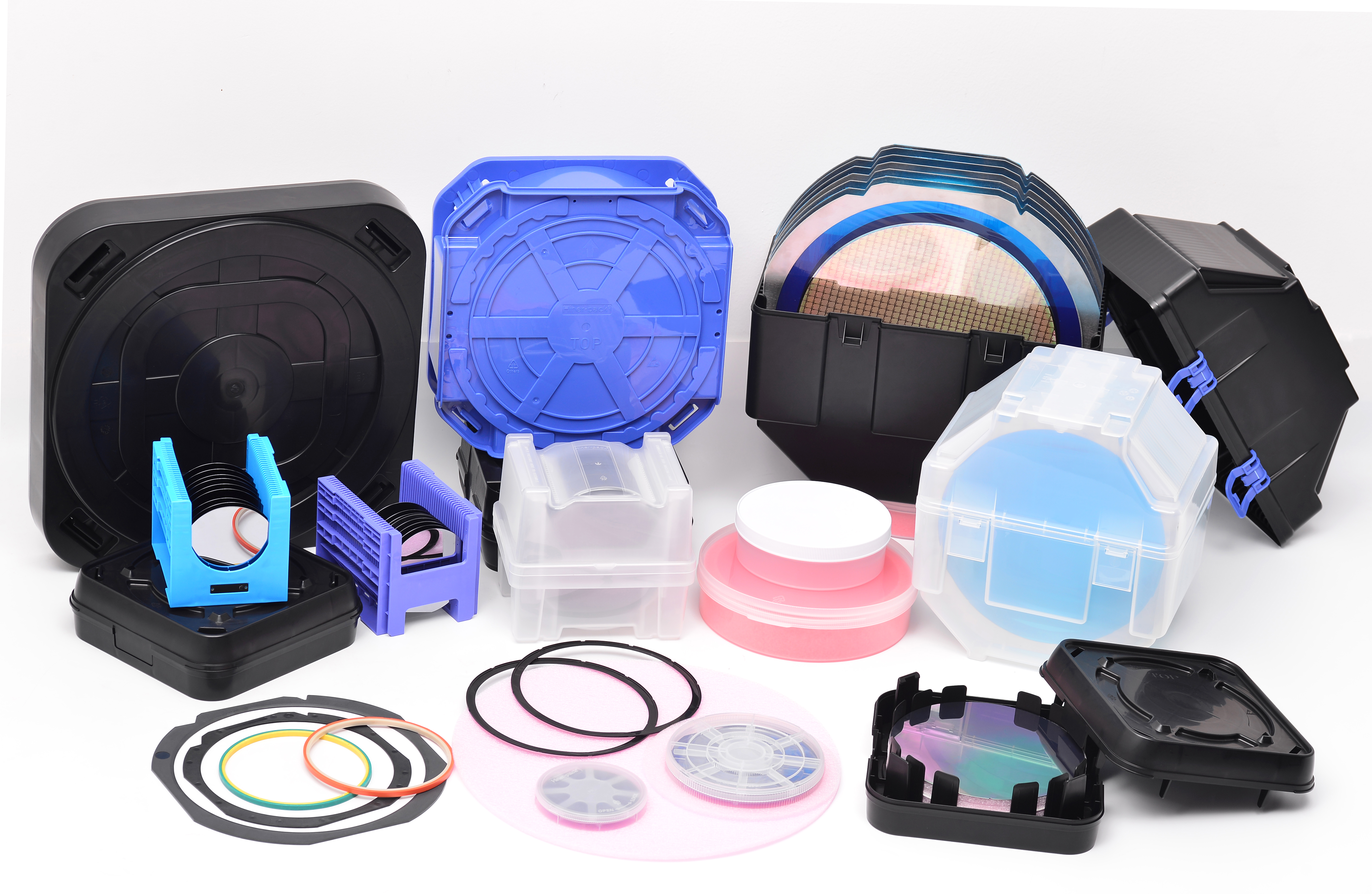
1. The Distinct Roles of FOSB and FOUP
It is vital to distinguish between the two primary types of carriers used for 12-inch wafers. While they look similar, their engineering tolerances and intended environments differ significantly.
The FOSB (Front Opening Shipping Box) is designed primarily for the transport of raw polished wafers from the silicon wafer manufacturer to the fab. The emphasis here is on shock absorption and seal integrity during truck or air transport.
The FOUP (Front Opening Unified Pod) is the standard for in-fab processing. These 300mm wafer carriers must interface seamlessly with the Automated Material Handling Systems (AMHS) and the load ports of process tools.
Mixing these up can be disastrous. A FOSB generally lacks the precise kinematic coupling required for high-precision tool docking. Conversely, a FOUP is often too expensive and heavy to be used as a disposable shipping container. Procuring the right type for the specific stage of the lifecycle is the first step in inventory management.
2. Kinematic Coupling and Robotic Precision
The bottom of a 300mm carrier features a specific arrangement of slots and grooves known as kinematic coupling pins. This is the most critical interface on the entire unit.
When an Overhead Hoist Transport (OHT) vehicle drops a carrier onto a load port, it must seat perfectly. The tolerance here is often measured in microns. If the coupling plate on the carrier is worn or poorly molded, the pod will sit at a slight angle.
This misalignment prevents the process tool from successfully opening the door. It triggers an alarm, halts the tool, and requires manual intervention. In a "lights-out" fully automated fab, these micro-stoppages destroy throughput efficiency.
High-quality 300mm wafer carriers use reinforced materials in this bottom plate area to resist wear from repeated docking cycles. We advise regular inspection of these coupling points to prevent unexpected docking failures.
3. Advanced Material Science: Controlling Outgassing
The plastic used in carrier manufacturing is not standard injection-molding grade. It must be chemically inert.
As line widths shrink to 5nm and 3nm nodes, the risk of molecular contamination increases. Standard plastics can release volatile organic compounds (outgassing) over time. If these molecules settle on the wafer surface, they can create "haze" or interfere with sensitive deposition layers.
Top-tier carriers utilize specialized Polycarbonate or PEEK (Polyether ether ketone) blends. These materials are chosen for their low outgassing properties and high thermal stability.
Furthermore, the material must block UV light. Many photoresists used in lithography are sensitive to specific wavelengths. Amber or orange-tinted carriers are standard to filter out UV radiation while still allowing operators to visually confirm the presence of wafers inside.
4. The Importance of Door Latch Reliability
The front door of a FOUP or FOSB is the only moving part that engages with the tool. It contains a complex mechanism of latch keys that lock the door into the carrier frame.
During processing, a tool’s opener mechanism inserts keys into the door, rotates them, and pulls the door inward to access the wafers. If the internal springs or cams inside the carrier door are stiff or broken, the handoff fails.
A jammed door is a nightmare scenario. It often results in wafers being trapped inside a tool or, worse, the door detaching mid-transport.
Reliable 300mm wafer carriers undergo rigorous cycle testing on these latch mechanisms. At Hiner-pack, we emphasize the durability of these moving parts. A carrier is only as good as its ability to open and close smoothly, thousands of times over its lifespan.
5. Moisture Control and Purge Capabilities
Oxygen and humidity are enemies of exposed copper interconnects. Oxidation can occur rapidly if wafers sit in a carrier queueing for the next process step.
To combat this, modern FOUPs are equipped with purge ports. These ports allow the AMHS or the docking station to inject nitrogen or clean dry air into the carrier, displacing the oxygen and moisture.
The seal integrity of the carrier is paramount here. The gasket running around the door frame must maintain a hermetic seal to keep the nitrogen in and the ambient fab air out. Over time, these gaskets can compress or crack.
Regular maintenance involves checking these seals. A leaky carrier wastes nitrogen and fails to protect the critical film layers on the wafer.
6. Managing Static Electricity (ESD)
Movement creates friction, and friction creates static. In a dry cleanroom environment, a plastic box moving on a conveyor is a static generator.
If a 300mm wafer accumulates charge, it becomes a magnet for airborne particles. A single particle landing on a critical die area kills the chip. Worse, a discharge event can vaporize the microscopic circuitry.
Effective 300mm wafer carriers incorporate carbon powder or carbon nanotubes into the polymer matrix. This makes the carrier "static dissipative." It provides a controlled path for the electrical charge to bleed off to the ground through the equipment load port.
It is not enough to simply coat the surface. Surface coatings wear off. The ESD protection must be intrinsic to the material itself to ensure safety throughout the carrier's years of service.
7. Weight Consistency and Balance
A fully loaded carrier with twenty-five 300mm silicon wafers weighs roughly 9 to 10 kilograms.
Robotic arms and OHT vehicles are programmed with specific torque and speed parameters based on this weight. If the carrier itself varies significantly in weight due to poor manufacturing consistency, it can throw off the center of gravity.
This imbalance leads to excessive vibration during transport. While silicon is hard, it is brittle. Vibration causes wafers to rattle in their slots. This rattling generates microscopic silicon dust—particles that come from the wafer itself and contaminate the active surface.
High-precision molding ensures that every carrier has an identical mass distribution. This consistency allows the automation systems to move at maximum speed without inducing dangerous vibrations.
8. Hiner-pack’s Role in Supply Chain Stability
The semiconductor industry is cyclical, but the demand for consumables is constant. A shortage of carriers can bottleneck a fab just as easily as a shortage of photoresist.
Procurement teams often face long lead times from the major OEM giants. This is where Hiner-pack steps in. We focus on providing high-specification carrier solutions that align with international standards, ensuring that your fab never stops due to a lack of logistics hardware.
We understand that you need options that bridge the gap between cost-effectiveness and strict technical compliance. By focusing on robust materials and precise molding tolerances, we help fabs maintain their OEE (Overall Equipment Effectiveness).
9. Cleaning and Lifecycle Management
Carriers are reusable assets, but they require care. They accumulate dust and residues over time.
Fabs utilize specialized carrier wash tools. These machines use deionized water and surfactants to clean the pods. The plastic material must be able to withstand these wash cycles without absorbing water or becoming brittle.
However, no carrier lasts forever. A robust tracking system, usually involving RFID tags or barcodes, is necessary to track the cycle count of each unit.
Fab managers should establish a protocol for retirement. Once a carrier reaches a certain number of cycles, or if the kinematic coupling shows visible wear, it should be downgraded or scrapped. Using a "retired" carrier for critical process steps is a false economy.
10. The Slot Pitch and Wafer Support
Inside the carrier, the wafers rest on teeth or shelves. The standard pitch (distance between wafers) for 300mm is 10mm.
The geometry of these teeth is engineered to minimize contact area. We want to hold the wafer securely but touch it as little as possible to reduce particle generation.
The "slump" factor is also real. 300mm wafers are large and can sag slightly under their own weight if not supported correctly. The teeth in the 300mm wafer carriers must extend far enough to support the wafer edge without obscuring the robotic end-effector that needs to slide underneath to pick up the wafer.
This balance between support and accessibility is the result of precise engineering design.
The evolution of the semiconductor industry is a story of precision. Every component in the fab, down to the plastic box carrying the wafers, must perform without error.
300mm wafer carriers are integral to the yield and profitability of modern manufacturing. From ESD protection and material purity to kinematic precision and latch durability, the specifications of these pods directly impact your bottom line.
Do not overlook the importance of your logistics hardware. Choosing a reliable partner ensures that your expensive silicon remains safe from the fab floor to the final customer. At Hiner-pack, we are committed to delivering the quality and consistency your process requires.
Frequently Asked Questions (FAQ)
Q1: What is the main difference between a FOSB and a FOUP?
A1: A FOSB (Front Opening Shipping Box) is designed for shipping wafers between facilities, focusing on shock protection and secure packing. A FOUP (Front Opening Unified Pod) is designed for internal fab processing, featuring high-precision interfaces for automated tool docking and purging capabilities.
Q2: How many wafers does a standard 300mm carrier hold?
A2: The industry standard capacity for 300mm wafer carriers is 25 wafers. The slots are numbered 1 through 25, usually starting from the bottom up, with a standard pitch of 10mm between wafers.
Q3: Can 300mm carriers be repaired if the door latch breaks?
A3: In some cases, yes. The door is often a separate assembly from the main body (shell). If the shell is intact, the door can sometimes be replaced or the latch mechanism repaired. However, if the kinematic coupling on the bottom of the shell is damaged, the carrier typically needs to be scrapped to avoid machine alignment errors.
Q4: Why are most 300mm carriers colored orange or amber?
A4: The amber or orange color is a specific UV-blocking tint. It filters out ultraviolet light that could damage UV-sensitive photoresists present on the wafers during lithography processes, while still allowing operators to see inside the carrier to verify wafer inventory.
Q5: How often should 300mm wafer carriers be cleaned?
A5: Cleaning frequency depends on the specific fab protocols and the process stage. Generally, carriers are washed after every few loops through the fab or if they have been used in "dirty" process steps (like CMP or copper plating). RFID tags track these cycles to ensure no carrier skips a scheduled wash.


