
Shipping 200mm, 300mm, or 450mm wafers requires packaging that balances mechanical protection, electrostatic discharge (ESD) control, and particle cleanliness. Injection‑molded shippers have been the standard, but a vacuum-formed wafer shipper offers distinct advantages for low‑to‑medium volume production, prototype shipments, and custom geometries. This guide examines seven engineering parameters where vacuum forming outperforms traditional methods. Each point is grounded in SEMI standards and cleanroom validation data.
1. Rapid Tooling and Low Initial Investment
Injection molds for a conventional wafer shipper cost $30,000–$80,000 and take 12–16 weeks. A vacuum-formed wafer shipper uses aluminum or epoxy tooling that costs $3,000–$8,000 and is ready in 3–4 weeks. This speed benefits:
Prototype runs for new wafer sizes (e.g., 200mm to 300mm transition).
Short‑run specialty devices (MEMS, power semiconductors, GaAs).
Customer‑specific cavity configurations with custom foam or gel inserts.
Hiner-pack offers low‑volume vacuum forming for fabs that cannot justify high injection mold costs. Tooling modifications are also cheaper – a pocket redesign costs under $1,000 vs. $10,000+ for injection molds.
2. Material Selection for Conductivity and Cleanliness
Vacuum forming works with a range of thermoplastic sheets. For a vacuum-formed wafer shipper, common materials include:
Conductive polycarbonate (PC) – surface resistivity 10³–10⁵ ohms/sq, Tg 147°C, good impact strength.
Static dissipative ABS – resistivity 10⁶–10⁹ ohms/sq, lower cost but less temperature resistance.
Carbon‑filled PETG – clarity allows visual inspection, resistivity stable after forming.
Material thickness typically ranges from 0.5 mm to 3.0 mm. Thinner gauges reduce weight and cost but require careful design to avoid flexing. Conductive wafer carriers and accessories made by vacuum forming can achieve particle counts below ISO Class 4 when proper sheet handling is used.
3. Dimensional Accuracy and Warpage Control
A common concern about vacuum forming is part warpage. Modern vacuum formers with heated platens and controlled cooling cycles achieve tolerances of ±0.15 mm over 300 mm length. For a vacuum-formed wafer shipper, this is sufficient for wafer support ribs that contact only the outer 3 mm exclusion zone.
Use FEM simulation to predict shrinkage (typically 0.5–0.8% for PC).
Add draft angles (1–2°) to facilitate part removal without distortion.
Post‑form annealing (80°C for 2 hours) relieves residual stresses and reduces warpage by 60%.
SEMI E154 specifies warpage limit of 0.5 mm for 300 mm shippers. Hiner-pack validates each production batch with a coordinate measuring machine (CMM) to ensure compliance.
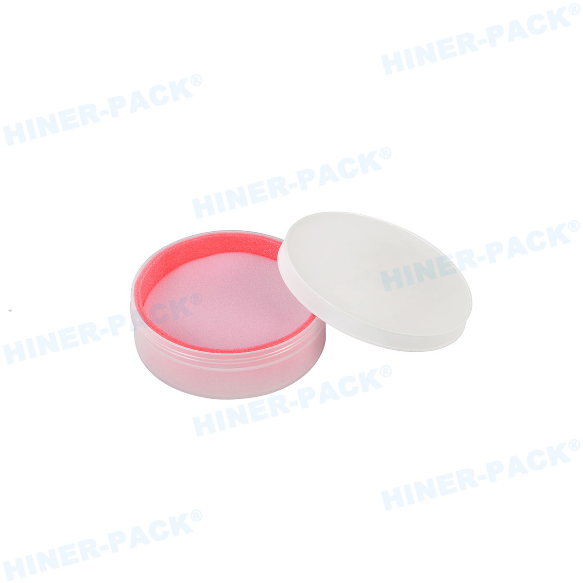
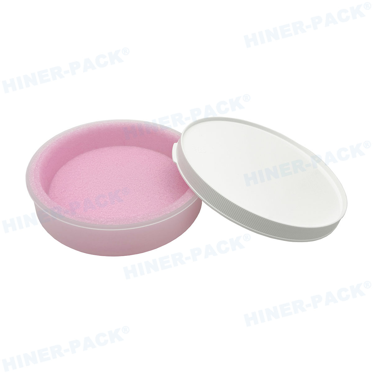
4. Integration of Foam and Gel Cushioning
Unlike injection‑molded rigid designs, vacuum‑formed shippers easily accept secondary assembly of cushioning layers. Typical configurations:
Conductive polyurethane foam – die‑cut to match wafer pockets, compression set < 5% after 1,000 cycles.
Thermoplastic elastomer (TPE) gel pads – self‑healing properties, ideal for fragile wafers (50 µm thickness).
Anti‑static corrugated inserts – low cost for single‑use shipments.
A vacuum-formed wafer shipper with foam inserts passes ISTA 3A vibration tests (0.5–2 Grms) and 50g shock tests. The vacuum‑formed shell provides rigid backbone while the foam absorbs energy.
5. Particle Performance and Cleanroom Compatibility
Particle generation from the shipper is a top concern. Vacuum‑formed parts can meet ISO Class 4 (Class 10) if the sheet material is cleanroom‑grade and the forming process is controlled. Key factors:
Use virgin resin (no regrind) to avoid contaminants.
Form in a cleanroom environment (ISO 7 or better) with HEPA‑filtered air.
Post‑form cleaning: ultrasonic wash in DI water + 70% IPA rinse, then dry in a laminar flow oven.
Independent testing of a vacuum-formed wafer shipping tray from Hiner-pack showed particle counts below 10 particles ≥0.3 µm per cm², meeting SEMI F57 requirements.
6. ESD Performance Consistency After Forming
Thermoforming can change the surface resistivity of conductive materials due to polymer chain orientation. For a vacuum-formed wafer shipper, verify that resistivity stays within 10³–10⁵ ohms/sq after forming. Carbon‑filled PC typically maintains its conductivity because the carbon network is not disrupted by stretching.
Test at three locations: flat bottom, sidewall, and deep-drawn pocket.
Use a concentric ring probe (ASTM D257) with 10V applied.
Acceptable variation: ≤ 0.5 decade from specification.
Static decay time (per ESD STM12.1) should be < 0.1 second for conductive materials. Hiner-pack provides a resistivity map for every shipper lot.
7. Cost‑Benefit for Low‑Volume and Mixed‑Size Shipments
For fabs shipping fewer than 500 shippers per month, injection molding is often uneconomical. A vacuum-formed wafer shipper reduces per‑unit cost by 40–60% at volumes of 100–5,000 pieces per year. Additional savings come from:
Lower inventory holding costs (fast tooling allows just‑in‑time production).
Easy design iterations for new wafer maps or notched orientations.
Combination shippers that hold two different wafer sizes in one tray.
Mixed‑size capability is especially valuable for R&D fabs and university cleanrooms. A single vacuum‑formed base can accept interchangeable inserts for 150mm, 200mm, and 300mm wafers.
Case Study: MEMS Fab Reduces Shipper Cost by 55%
A MEMS manufacturer needed 2,400 shippers per year for 200mm wafers. Injection molding would have cost $38,000 for tooling plus $12 per unit. Hiner-pack proposed a vacuum-formed wafer shipper with conductive PC. Tooling cost: $5,200. Per‑unit cost: $6.50. Total first‑year savings exceeded $20,000. Particle and ESD tests passed SEMI specifications. The fab now uses vacuum‑formed shippers for all low‑volume product families.
Frequently Asked Questions (FAQ)
Q1: What is the maximum wafer size that can be accommodated by a
vacuum-formed wafer shipper?
A1: Vacuum forming can produce shippers
for wafers up to 450mm. The limiting factor is sheet size and forming depth. For
450mm, a sheet of 600mm x 600mm with 3mm thickness is required. Forming depth
for pockets should not exceed 1:1 draw ratio to avoid thinning. Most suppliers,
including Hiner-pack, support
450mm designs with SEMI E158 compliance.
Q2: How many cleaning cycles can a vacuum-formed wafer shipper
withstand?
A2: With proper material selection (polycarbonate), a
shipper can survive 50–100 cleaning cycles using ultrasonic baths with mild
detergent or 70% IPA. After each cycle, inspect for crazing, warpage, and
resistivity drift. Polycarbonate is more resistant than PETG or ABS. For
high‑cycle applications, consider injection‑molded shippers, but for most
low‑volume fabs, vacuum‑formed units are cost‑effective.
Q3: Can a vacuum-formed wafer shipper include RFID or barcode
features?
A3: Yes. A recess pocket can be formed into the base or
lid to accept a pre‑molded RFID inlay or adhesive barcode label. The pocket
depth should be 1.5–2.0 mm with a retaining ridge. Ensure that the label
material is cleanroom‑compatible and ESD‑safe. Custom wafer shipping
accessories like RFID pockets are common vacuum‑formed features.
Q4: What is the typical lead time for a custom vacuum-formed wafer
shipper?
A4: Tooling fabrication takes 2–4 weeks. First article
samples are available in 3–5 weeks. After approval, production quantities
(500–2,000 units) ship in 2–3 weeks. This is significantly faster than injection
molding (16–20 weeks total). Expedited tooling (1 week) is possible for simple
designs but costs 30–50% more.
Q5: Are vacuum-formed wafer shippers compatible with automated wafer
handling equipment (load ports, robots)?
A5: Yes, but precision is
required. The shipper’s outer dimensions and kinematic coupling features (SEMI
E15.1) can be vacuum‑formed if draft angles are small (< 2°) and material
thickness is uniform. However, for high‑precision automated fabs (Class 1
automation), injection‑molded shippers may offer better repeatability. For
semi‑automated or manual load ports, vacuum‑formed shippers work reliably. Hiner-pack can add
machined kinematic pads to a vacuum‑formed base for automation
compatibility.
Request a Design Consultation or Sample Quote
Selecting the right vacuum-formed wafer shipper requires balancing cost, lead time, and cleanroom performance. Hiner-pack provides free engineering reviews for your wafer size, quantity, and handling environment. Send your wafer map, desired ESD properties, and annual volume. We will return a full proposal including material recommendations, tooling cost, per‑unit price, and particle test data from a representative sample.
Submit an inquiry to our semiconductor packaging team → Click here for a response within 24 hours


