
Shipping 300mm and 200mm wafers between fabs or to assembly sites requires more than a plastic box. A conductive wafer shipper must control electrostatic discharge (ESD), maintain particle cleanliness, and withstand vibration. Many incidents of device damage trace back to improper shipper selection. This guide presents eight measurable parameters that procurement and process engineers should verify before purchasing. Each point is derived from SEMI standards and field failure analysis.
1. Surface Resistivity Range and ESD Control
The primary function of a conductive wafer shipper is to prevent charge accumulation. SEMI E78 and ANSI/ESD S20.20 require surface resistivity between 10³ and 10⁵ ohms/sq for conductive materials. Resistivity below 10³ ohms/sq risks galvanic corrosion or charge bleed-off that may damage sensitive devices.
Measure resistivity with a concentric ring probe (ASTM D257 method).
Check that the material is homogeneous – not just a coated surface that can wear off.
Avoid shippers that rely on antistatic additives that migrate or deplete over time.
Hiner-pack engineers recommend testing shippers after each cleaning cycle to verify that resistivity remains within specification.
2. Particle Generation and Cleanliness Class
Wafer shippers must meet ISO Class 4 or better (Fed-Std-209E Class 10). Particles from the shipper material can transfer to wafer surfaces, causing killer defects. Key factors:
Material composition – polycarbonate (PC) blended with carbon nanotubes generates fewer particles than carbon-fiber filled materials.
Molded-in vs. post-applied conductive layers – molded-in conductive fillers have lower sloughing.
Ask for a particle count report using liquid particle counting (LPC) per IEST-STD-CC1246.
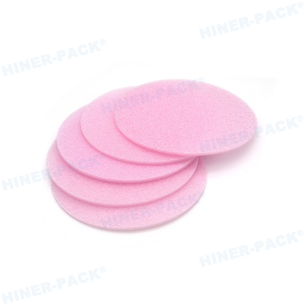
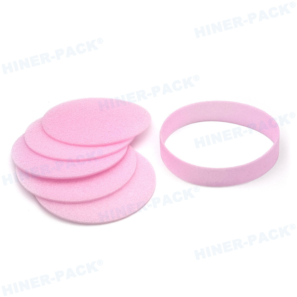
For high-value devices (automotive, medical), a conductive wafer shipper should also include a lint-free foam insert or gel pack to cushion wafers without shedding.
3. Outgassing and Chemical Compatibility
Outgassing from shipper materials can corrode aluminum pads or contaminate wafer surfaces. SEMI S2 and SEMI S6 require evaluation of volatile organic compounds (VOCs).
Request an outgassing test per SEMI F57 (dynamic headspace GC-MS).
Limit for total VOCs: ≤ 0.5 µg/g for class 10 cleanroom applications.
Avoid materials containing plasticizers (e.g., phthalates) or halogenated flame retardants.
Polypropylene (PP) and polycarbonate (PC) grades designed for cleanroom use are preferred. wafer shipping accessories like foam inserts must also pass outgassing tests.
4. Mechanical Shock and Vibration Damping
During air or ground transport, wafers experience random vibration (0.5–2 Grms) and shock (up to 50g). A conductive wafer shipper must hold wafers securely without edge contact.
Look for wafer support ribs that contact only the outer 3mm of the wafer (exclusion zone).
Compression foam gaskets or gel pads should provide 2–5 mm of preload.
Verify ISTA 3A or ASTM D4169 compliance (package performance testing).
Check that the shipper’s latch mechanism does not allow lid deflection. A weak latch can cause wafers to bounce and crack. Hiner-pack provides drop test reports for each shipper design.
5. Moisture Barrier and Humidity Control
Many semiconductor devices are moisture-sensitive (MSL rating). A conductive wafer shipper alone does not provide hermetic seal, but it can be combined with moisture barrier bags (MBB) and desiccants.
Shipper material should have low water absorption (≤ 0.2% for PC, ≤ 0.01% for PP).
Integral foam gaskets should not retain moisture after dry‑baking.
For long‑term storage, choose a shipper that accepts a humidity indicator card (HIC) and desiccant pouch.
Evaluate the sealing force of the lid – a 5‑psi differential pressure should not cause leakage. Some designs include a silicone seal groove.
6. Dimensional Stability and Warpage Tolerance
Warpage of the shipper base or lid leads to uneven wafer support and potential breakage. Thermal cycling during transport (‑40°C to +60°C) can distort low‑grade polymers.
Specify maximum warpage: ≤ 0.5 mm over 300 mm length per SEMI E154.
Material must have glass transition temperature (Tg) above 120°C for polycarbonate, or 80°C for polypropylene.
Ask for thermal cycling test data (100 cycles from ‑40°C to +85°C with no permanent deformation).
Conductive wafer carriers and accessories from Hiner-pack include FEA (finite element analysis) reports to verify structural rigidity.
7. Compatibility with Automated Handling Equipment
Fabs use robotic end effectors and load ports (e.g., SEMI E15.1). The shipper must have precise locating features.
Check for SEMI standard kinematic coupling features (three ball sockets or v‑grooves).
Outer dimensions must conform to SEMI E47 (FOUP and FOSB sizes).
RFID or barcode label recess should be present for traceability.
A conductive wafer shipper without proper automation features will cause jams and downtime. Request a dimensional report per SEMI E1.9.
8. Cleanroom Washability and Chemical Resistance
Shippers must survive repeated cleaning cycles (DI water, IPA, or ultrasonic baths) without degradation. Material compatibility with common fab cleaning agents is mandatory.
Test resistance to 70% IPA, acetone (short exposure), and mild alkaline detergents.
No surface crazing or loss of conductivity after 50 cleaning cycles.
Check that the carbon conductive network does not leach out (visual inspection for black residue on wipes).
Hiner-pack provides a cleaning validation protocol for its shippers, including surface resistivity checks after each cleaning cycle.
Case Example: Reducing ESD Failures from 4% to 0.2%
A MEMS fab experienced intermittent gate oxide failures after shipment. Investigation revealed that the existing conductive wafer shipper had surface resistivity above 10⁸ ohms/sq due to wear. Hiner-pack supplied a carbon‑filled PC shipper with verified 10⁴ ohms/sq and integrated conductive foam. ESD‑related failures dropped to 0.2%, saving $400,000 annually in scrap.
Frequently Asked Questions (FAQ)
Q1: How do I measure the surface resistivity of a used conductive
wafer shipper?
A1: Use a portable resistance meter with concentric
ring probes (e.g., ACL 800 or Prostat PRS-801). Place probes on a clean, dry
area of the shipper interior. Apply 10V or 100V depending on material.
Acceptable range for conductive shippers: 10³ to 10⁵ ohms/sq. Readings above 10⁵
indicate material degradation.
Q2: Can a conductive wafer shipper be recycled or returned to the
supplier?
A2: Yes, many suppliers including Hiner-pack operate
return‑and‑reuse programs. Shippers are washed, inspected for cracks and
resistivity, then recertified. This reduces cost per shipment and meets
sustainability goals. Always confirm that recycled shippers have valid particle
and outgassing data.
Q3: What is the difference between conductive, static dissipative,
and antistatic wafer shippers?
A3: Conductive: 10³–10⁵ ohms/sq,
allows rapid charge bleed. Static dissipative: 10⁵–10¹¹ ohms/sq, slower
discharge but prevents sudden spark. Antistatic: 10¹¹–10¹⁴ ohms/sq, only reduces
triboelectric charging. For sensitive devices (MOSFETs, GaAs), conductive is
mandatory. Always match the shipper to device sensitivity per ANSI/ESD
STM5.1.
Q4: How often should I replace conductive wafer
shippers?
A4: Depending on usage frequency and cleaning cycles. For
weekly shipments, inspect every 6 months for resistivity drift, cracks, or foam
compression set. Replace after 50‑100 cleaning cycles or when surface
resistivity exceeds 10⁵ ohms/sq. Some high‑durability shippers last 3–5 years
with proper care.
Q5: Are there special requirements for shipping 450mm
wafers?
A5: Yes, 450mm wafers require larger form factor shippers
(SEMI E158). The conductive material must handle higher mass and different
vibration modes. Few suppliers offer certified 450mm solutions. Consult specialized wafer shipping
accessories providers like Hiner‑pack for custom designs.
Request a Technical Consultation or Sample Evaluation
Choosing the wrong conductive wafer shipper leads to device failures, yield loss, and customer returns. Hiner-pack offers free sample evaluation for qualified fabs. Send your wafer size, device sensitivity, and shipment volume (units/month). Our engineering team will provide resistivity test reports, particle data, and a compatibility matrix with your automated handling systems.
Submit an inquiry to our semiconductor logistics team → Click here for a response within 24 hours


