
In the high-stakes world of semiconductor manufacturing and logistics, every component's journey matters. From wafer fabrication to final assembly, protecting delicate integrated circuits (ICs) and chips is non-negotiable. This is where standardized packaging becomes critical. Among the most trusted solutions are Plastic JEDEC trays. These precision-engineered carriers are the unsung heroes of the electronics supply chain, ensuring components arrive intact, organized, and ready for automated assembly. Their design, governed by global standards, guarantees compatibility and reliability across a fragmented industry.
For companies like Hiner-pack, specializing in high-performance semiconductor packaging, understanding and utilizing the right Plastic JEDEC trays is fundamental to delivering value and protection to clients worldwide.
What Exactly Are Plastic JEDEC Trays?
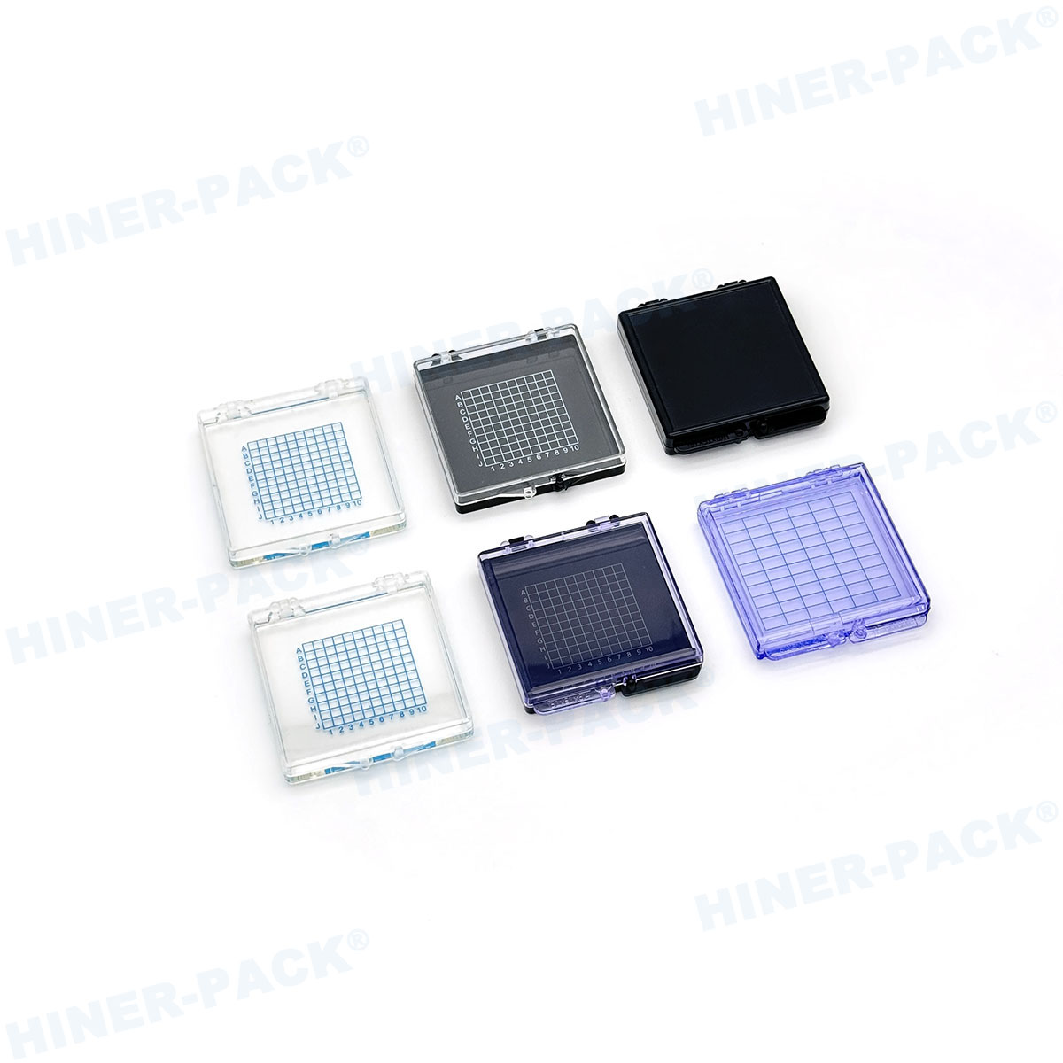
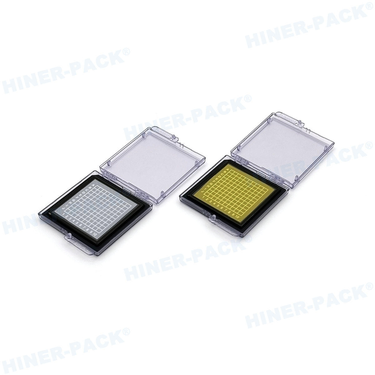
Plastic JEDEC trays are standardized carrier trays used for handling, transporting, and shipping semiconductor devices such as integrated circuits, transistors, and other surface-mount components. They conform to specifications set by JEDEC (Joint Electron Device Engineering Council), the global semiconductor standardization body.
This standardization dictates precise dimensions, cavity layouts, and material properties. The goal is interoperability. A tray filled at a factory in Asia should seamlessly fit into the automated handling equipment at an assembly plant in Europe or the Americas. This eliminates costly mismatches and delays.
Common materials include conductive, dissipative, or anti-static polycarbonate (PC), polyetheretherketone (PEEK), and acrylonitrile butadiene styrene (ABS). The choice depends on the required level of electrostatic discharge (ESD) protection and mechanical durability.
How to Choose the Right Plastic JEDEC Tray
Selecting the correct tray is not a one-size-fits-all decision. Several technical factors must align with your process.
First, identify the exact JEDEC outline. Standards like MO-047, MO-095, or MO-150 define the tray’s footprint and cavity pattern. Matching your device’s dimensions to this outline is the first step.
Next, consider ESD requirements. For sensitive components, trays with a surface resistivity of 10^5 to 10^11 ohms/sq (dissipative) are essential to safely ground any static charge. Conductive trays offer even lower resistance.
Material rigidity and temperature resistance are crucial. Trays must withstand repeated use and potential exposure to high temperatures during baking or curing processes. Hiner-pack’s high-temp PC trays, for instance, are designed for such demanding environments.
Finally, evaluate features like stackability, robot pick-up flanges, and compatibility with tape-and-reel equipment. A well-chosen tray integrates smoothly into your entire production line.
Top Benefits of Using Standardized JEDEC Trays
The adoption of these trays brings tangible operational advantages that directly impact the bottom line.
The primary benefit is unparalleled protection. Custom cavities cradle each device, preventing mechanical damage from scratching, chipping, or bending leads during transit and handling. This drastically reduces yield loss.
They enable high-volume automation. Standard dimensions allow robotic arms to quickly pick and place components from the trays onto printed circuit boards (PCBs). This speeds up assembly and reduces human error.
Inventory management and logistics become simpler. Standard trays stack securely, maximizing space in storage and shipping containers. Their uniformity allows for easy counting and tracking of components.
Compliance and traceability are enhanced. Using industry-standard carriers ensures compliance with customer and industry requirements. Many trays can also be labeled with barcodes for full lot traceability.
Ultimately, they reduce total cost. While there's an initial purchase, the reduction in damaged components, improved handling efficiency, and streamlined processes lead to significant long-term savings.
Critical Applications in the Semiconductor Industry
Plastic JEDEC trays are ubiquitous across the chip lifecycle. Their role is vital in several key stages.
In post-fabrication, trays transport singulated chips from dicing saws to testing facilities. They protect the bare die or packaged units during electrical testing and qualification.
During IC packaging, trays hold devices through processes like trim-and-form, marking, and final inspection. They are the standard carrier between these discrete manufacturing steps.
In logistics and distribution, trays are the preferred method for shipping high-pin-count or sensitive components to contract manufacturers (CMs) and original equipment manufacturers (OEMs). A shipment from Hiner-pack to a customer typically involves these secure trays.
For board assembly, trays feed pick-and-place machines directly, especially for large, complex, or odd-shaped components not available on tape and reel.
Hiner-pack's Approach to Tray Manufacturing and Innovation
At Hiner-pack, we view Plastic JEDEC trays as precision tools, not just containers. Our manufacturing process emphasizes consistency and quality.
We start with certified raw materials that meet strict ESD and mechanical specs. Our molding processes are controlled to produce trays with exacting tolerances, ensuring perfect cavity dimensions and flatness to prevent device pop-out or warpage.
We focus on durability. Our trays are engineered for hundreds of reuse cycles without degradation of ESD properties or physical structure, offering a better return on investment.
Innovation for us means addressing niche needs. We offer custom labeling areas, unique cavity modifications for specialized components, and tailored material blends for extreme environments, all while maintaining JEDEC-standard external dimensions for compatibility.
Maintaining and Handling Your JEDEC Trays
Proper care extends tray life and maintains performance. Regular cleaning is essential to remove dust and contaminants that can interfere with device seating or cause electrostatic issues.
Use approved ESD-safe cleaners and lint-free wipes. Avoid harsh solvents that can degrade the plastic or alter its surface resistivity.
Inspect trays frequently for physical damage like cracks, burrs, or warping. Damaged trays should be removed from circulation immediately as they can harm components.
Store trays in a controlled environment, away from direct sunlight and extreme temperatures. Stack them properly as designed to avoid stress deformation.
Implementing a managed cycle program, where trays are tracked, cleaned, and inspected at intervals, maximizes their lifespan and reliability in your production flow.
The Future of Component Carriers
The evolution of Plastic JEDEC trays continues alongside semiconductor technology. As devices become smaller and more complex, trays will need to accommodate finer pitches and more delicate structures.
Sustainability is a growing focus. The industry is exploring recyclable materials and closed-loop systems for tray reuse and recycling. Hiner-pack is actively involved in developing more eco-friendly material options without compromising performance.
Integration with Industry 4.0 is another trend. We foresee trays with embedded RFID tags for even smarter tracking through the supply chain, providing real-time data on location and environmental conditions.
The core principle, however, remains: providing a standardized, reliable, and protective physical interface for valuable semiconductors. As a foundational element of the global electronics infrastructure, the Plastic JEDEC tray will continue to be indispensable.
Frequently Asked Questions (FAQ)
Q1: What is the main difference between conductive and dissipative Plastic JEDEC trays?
A1: Conductive trays have a very low surface resistivity (typically below 10^5 ohms/sq) and provide a rapid path to ground for static charges. Dissipative trays have a higher resistivity (10^5 to 10^11 ohms/sq) and safely bleed off static charge at a slower, controlled rate. The choice depends on the specific ESD sensitivity of the components being handled.
Q2: Can Plastic JEDEC trays be used in high-temperature processes like IC baking?
A2: Yes, but only if they are specifically manufactured from high-temperature resistant materials like certain grades of polycarbonate (PC) or PEEK. Standard trays may warp or lose their ESD properties. Always specify your temperature requirements to your supplier, like Hiner-pack, to ensure you receive trays rated for the necessary thermal exposure.
Q3: How do I know which JEDEC outline number my component requires?
A3: The outline is typically determined by your component's package type and dimensions (e.g., QFP, BGA, SOIC). Your component datasheet or packaging specifications should list the recommended JEDEC outline. You can also consult with your tray supplier, providing them with the component's mechanical drawing for a definitive match.
Q4: Are these trays reusable, and for how many cycles?
A4: High-quality Plastic JEDEC trays from reputable manufacturers are designed for multiple reuse cycles. The exact number depends on the material, handling care, and process conditions. A well-maintained tray from a brand like Hiner-pack can often withstand 50 to 100+ cycles or more before showing significant wear, making them a cost-effective choice.
Q5: Why choose Hiner-pack for Plastic JEDEC trays over other suppliers?
A5: Hiner-pack combines strict adherence to JEDEC standards with a focus on material quality and manufacturing precision. We offer expert guidance on material selection for specific applications, ensure exceptional tray-to-tray consistency for automated handling, and provide robust customer support. Our commitment is to deliver trays that protect your components reliably throughout their journey.


