
In the highly precise world of semiconductor production, even the smallest components can make or break the entire process. Imagine a scenario where delicate silicon wafers—the heart of modern electronics—are transported across facilities without adequate protection. Contamination, physical damage, or misalignment could lead to catastrophic losses, costing millions and delaying critical projects. This is where the FOSB wafer carrier comes into play. As an indispensable tool in the semiconductor industry, the FOSB wafer carrier ensures that wafers remain secure, clean, and organized from fabrication to assembly. But what exactly is a FOSB wafer carrier, and why has it become a cornerstone of wafer handling systems? In this article, we delve into the intricacies of the FOSB wafer carrier, exploring its design, applications, and the pivotal role it plays in maintaining the integrity of semiconductor manufacturing. Whether you're an engineer, a supply chain manager, or simply curious about semiconductor logistics, understanding the FOSB wafer carrier is key to appreciating the seamless operation behind today's tech innovations.
What is a FOSB Wafer Carrier?
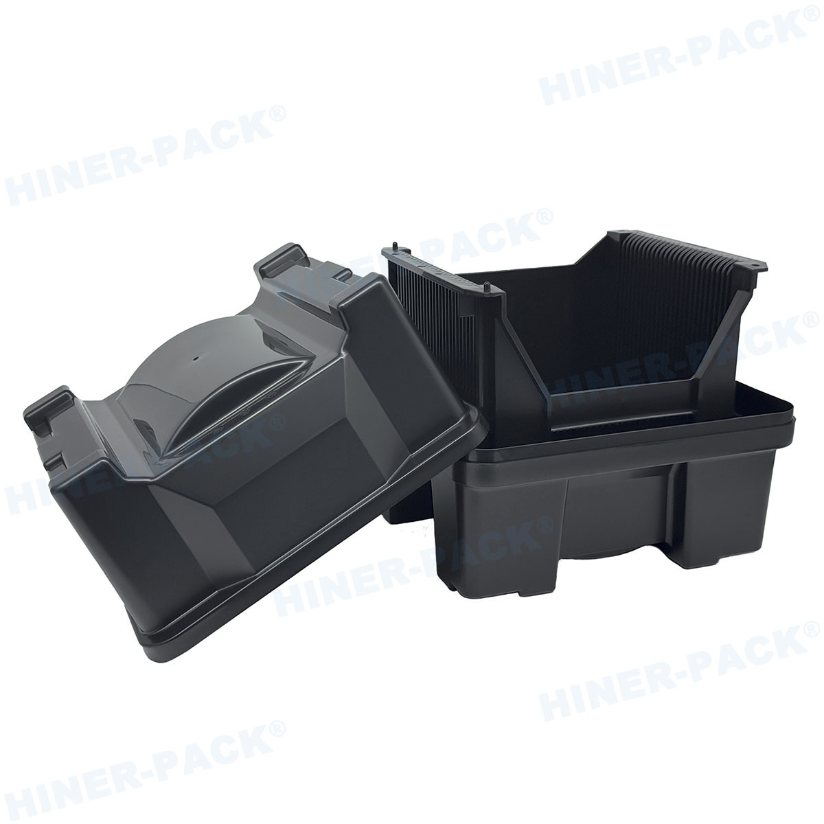
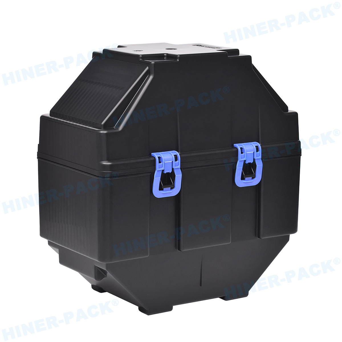
A FOSB wafer carrier, short for Front Opening Shipping Box, is a specialized container designed to hold and transport silicon wafers securely during various stages of semiconductor manufacturing. Unlike traditional carriers, the FOSB wafer carrier features a front-opening mechanism that allows for easy access to wafers while minimizing exposure to contaminants such as dust, moisture, and static electricity. This design is critical in environments like cleanrooms, where even microscopic particles can compromise wafer quality. Typically constructed from high-purity materials, the FOSB wafer carrier accommodates standard wafer sizes, such as 300mm, and includes features like precision slots and locking systems to prevent movement during transit. The evolution of the FOSB wafer carrier stems from the industry's need for standardized, reusable solutions that enhance safety and efficiency. By providing a controlled environment, the FOSB wafer carrier helps reduce defects and improve yield rates, making it a fundamental component in the semiconductor supply chain. Its adoption has grown rapidly due to compatibility with automated handling systems, which streamline processes in high-volume production facilities.
Design and Construction of FOSB Wafer Carriers
The design of a FOSB wafer carrier is a marvel of engineering, tailored to meet the stringent demands of semiconductor environments. At its core, the FOSB wafer carrier consists of a rigid frame made from materials like polycarbonate or other advanced polymers that offer high chemical resistance and low particulate generation. The front-opening door is a standout feature, often equipped with seals and latches that maintain an airtight closure, shielding wafers from external pollutants. Inside, the carrier includes precisely spaced slots that cradle each wafer individually, preventing contact and reducing the risk of scratches or breakage. Additionally, many FOSB wafer carriers incorporate RFID tags or barcodes for tracking purposes, enabling real-time monitoring throughout the logistics chain. The construction process involves injection molding and rigorous quality checks to ensure dimensional accuracy and durability. For instance, the internal surfaces are smooth and non-abrasive to avoid contaminating the wafers, while the overall structure is lightweight yet robust enough to withstand mechanical stress during shipping. This thoughtful design not only extends the lifespan of the FOSB wafer carrier but also supports sustainability efforts by allowing repeated use after proper cleaning. As semiconductor technology advances toward smaller nodes and larger wafers, the FOSB wafer carrier continues to evolve, integrating smart features like sensors for environmental monitoring.
Key Applications in the Semiconductor Industry
The FOSB wafer carrier finds its primary applications in the semiconductor industry, where it serves as a vital link between manufacturing steps. From wafer fabrication to testing and packaging, the FOSB wafer carrier ensures that wafers are transported safely between cleanrooms, fabrication plants, and assembly lines. In front-end processes, such as photolithography and etching, wafers must be moved without exposure to airborne particles; the FOSB wafer carrier's sealed design makes this possible. Similarly, in back-end operations like dicing and bonding, the carrier facilitates efficient handling by automated equipment, reducing manual intervention and the associated risks of human error. Beyond internal logistics, the FOSB wafer carrier is also used for inter-facility shipping, where it protects wafers from vibrations, temperature fluctuations, and humidity during transit. This versatility has made the FOSB wafer carrier a standard in foundries and OSAT (Outsourced Semiconductor Assembly and Test) facilities worldwide. Moreover, as the industry embraces trends like IoT and 5G, which demand higher wafer integrity, the role of the FOSB wafer carrier becomes even more critical. It supports just-in-time manufacturing models by enabling reliable, rapid transfers, thereby minimizing downtime and enhancing overall productivity.
Benefits of Using FOSB Wafer Carriers
Adopting the FOSB wafer carrier offers numerous benefits that directly impact operational efficiency and cost-effectiveness in semiconductor manufacturing. First and foremost, the FOSB wafer carrier provides superior protection against contamination, which is a leading cause of yield loss in wafer production. By maintaining a clean internal environment, it helps preserve the electrical properties of wafers, leading to higher-quality end products. Secondly, the front-opening design of the FOSB wafer carrier allows for easier loading and unloading compared to top-opening alternatives, speeding up processes and reducing the likelihood of damage during access. This ergonomic advantage is particularly valuable in automated systems, where the FOSB wafer carrier interfaces seamlessly with robots and conveyors. Thirdly, the reusability of the FOSB wafer carrier contributes to sustainability goals, as it minimizes waste compared to single-use packaging. With proper maintenance, a single FOSB wafer carrier can endure hundreds of cycles, offering long-term savings. Additionally, the standardization of the FOSB wafer carrier across the industry promotes interoperability, simplifying supply chain logistics and reducing compatibility issues. Finally, the integration of tracking technologies in modern FOSB wafer carriers enhances traceability, allowing manufacturers to monitor wafer history and optimize inventory management. Overall, the FOSB wafer carrier is a cost-efficient solution that balances performance with reliability.
Maintenance and Best Practices for FOSB Wafer Carriers
To maximize the lifespan and effectiveness of a FOSB wafer carrier, proper maintenance is essential. Regular cleaning is a cornerstone of upkeep, as residues from wafers or environments can accumulate and lead to contamination. Typically, the FOSB wafer carrier should be cleaned using specialized equipment, such as ultrasonic cleaners with deionized water and mild solvents, to remove particles without damaging the material. It's crucial to follow manufacturer guidelines for cleaning frequency and methods to avoid compromising the structural integrity of the FOSB wafer carrier. Inspection is another key practice; each FOSB wafer carrier should be checked for signs of wear, such as cracks, warping, or degraded seals, before reuse. Any damaged carriers must be removed from circulation to prevent wafer loss. Storage conditions also matter—the FOSB wafer carrier should be kept in a controlled environment, away from direct sunlight or extreme temperatures, to maintain its properties. When handling the FOSB wafer carrier, personnel should use proper PPE and adhere to cleanroom protocols to avoid introducing contaminants. Furthermore, implementing a rotation system for carriers can ensure even usage and extend their service life. By following these best practices, companies can uphold the high standards required for semiconductor manufacturing and get the most out of their investment in FOSB wafer carriers.
Future Trends and Innovations in FOSB Wafer Carriers
The future of the FOSB wafer carrier is shaped by ongoing advancements in semiconductor technology and the push for greater efficiency. One emerging trend is the integration of smart features into the FOSB wafer carrier, such as embedded sensors that monitor temperature, humidity, and shock in real-time. This data can be transmitted wirelessly to central systems, providing insights into transport conditions and enabling predictive maintenance. Another innovation involves the use of advanced materials, like carbon-fiber composites or antimicrobial coatings, to enhance the durability and cleanliness of the FOSB wafer carrier. As wafer sizes continue to increase—for example, with the industry exploring 450mm wafers—the FOSB wafer carrier will need to evolve in size and design to accommodate these changes while maintaining stability. Sustainability is also a driving force; researchers are developing recyclable and biodegradable versions of the FOSB wafer carrier to reduce environmental impact. Additionally, automation and AI are being leveraged to optimize the handling and tracking of FOSB wafer carriers, potentially leading to fully autonomous logistics networks. These innovations promise to make the FOSB wafer carrier even more integral to semiconductor manufacturing, supporting faster production cycles and higher yields in the years to come.
Frequently Asked Questions About FOSB Wafer Carriers
Q1: What does FOSB stand for in the context of wafer carriers?
A1: FOSB stands for Front Opening Shipping Box. It refers to a type of wafer carrier used in the semiconductor industry for safely transporting and storing silicon wafers. The front-opening design allows easy access while minimizing contamination risks.
Q2: How does a FOSB wafer carrier differ from other wafer carriers like FOUP?
A2: While both FOSB and FOUP (Front Opening Unified Pod) carriers have front-opening mechanisms, the FOSB wafer carrier is typically used for shipping and intermediate storage, often in less controlled environments, whereas FOUPs are designed for use within fabrication cleanrooms. FOSB carriers are generally more robust for external transit and may have simpler sealing systems.
Q3: What materials are commonly used in manufacturing FOSB wafer carriers?
A3: FOSB wafer carriers are commonly made from high-purity plastics such as polycarbonate or PEEK (polyether ether ketone), which offer excellent chemical resistance, low particulate generation, and durability. These materials ensure the carrier protects wafers from physical and environmental damage.
Q4: How often should a FOSB wafer carrier be cleaned and inspected?
A4: A FOSB wafer carrier should be cleaned after each use or according to the manufacturer's recommendations, typically using specialized cleaning processes to remove contaminants. Inspection for damage, such as cracks or wear, should occur before every reuse to maintain wafer integrity and safety.
Q5: Can FOSB wafer carriers be customized for specific wafer sizes or applications?
A5: Yes, FOSB wafer carriers can be customized to accommodate various wafer sizes, such as 200mm or 300mm, and specific application needs. Customizations may include adjusted slot configurations, additional shielding for sensitive wafers, or integrated tracking features to enhance logistics efficiency.


