In the fast-paced world of semiconductor manufacturing, every detail counts—from the intricate circuitry on silicon wafers to the containers that protect them. Wafer boxes for semiconductor applications are more than just storage units; they are critical components that safeguard delicate wafers from contamination, physical damage, and environmental factors during handling, transport, and storage. As the demand for smaller, more powerful chips grows, the importance of reliable wafer handling solutions cannot be overstated. Brands like Hiner-pack have emerged as trusted providers, offering innovative designs that meet the stringent requirements of the global semiconductor industry. In this article, we’ll explore practical solutions and insights to help you optimize your use of wafer boxes, ensuring efficiency and quality in your operations.
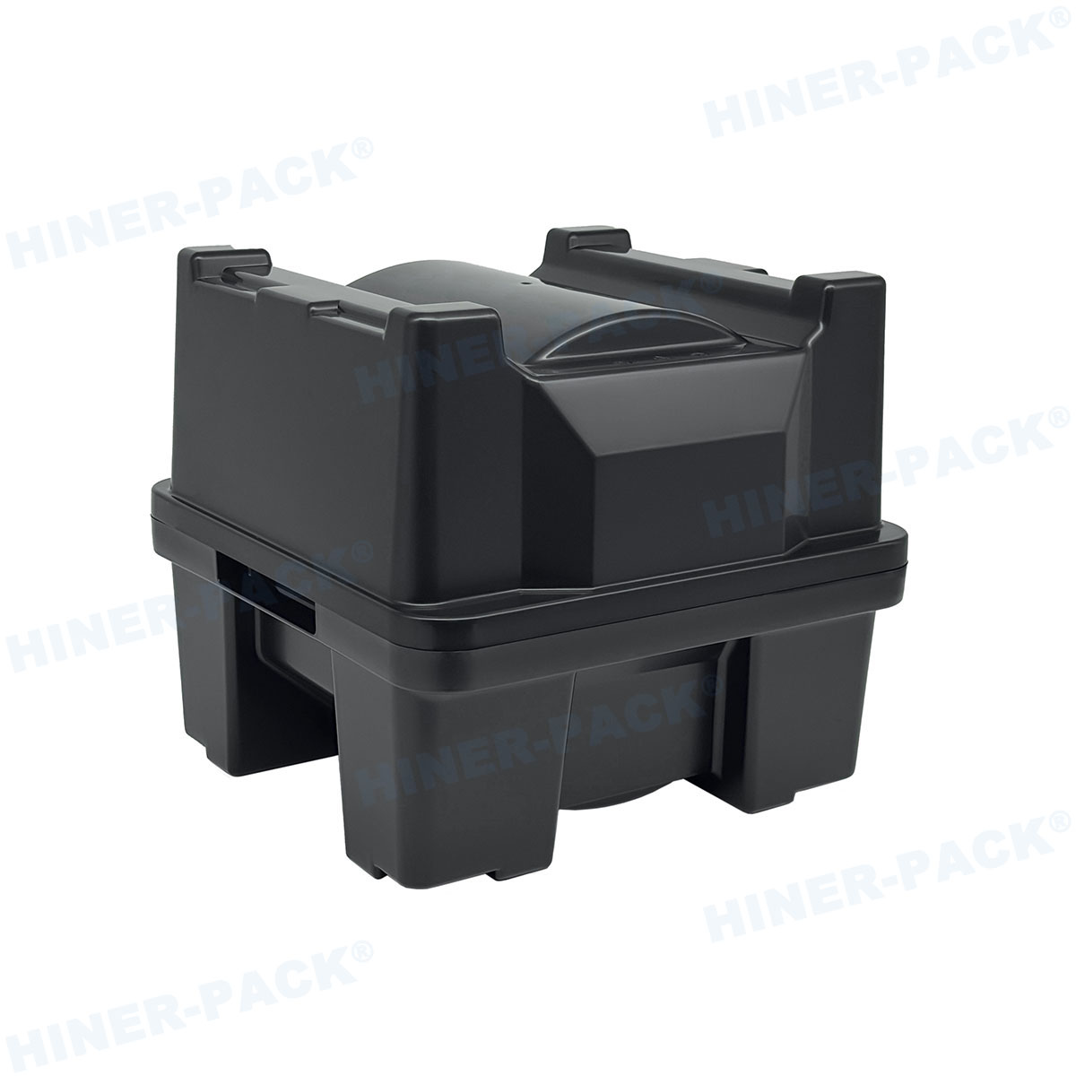
Wafer boxes, often referred to as wafer carriers or cassettes, are specifically engineered to hold semiconductor wafers securely. They come in various types, such as FOUPs (Front Opening Unified Pods) and FOSBs (Front Opening Shipping Boxes), each tailored for different stages of the manufacturing process. Whether you’re involved in fabrication, testing, or logistics, understanding how to leverage these containers can lead to significant cost savings and improved yield rates. Let’s dive into the key aspects that make wafer boxes for semiconductor applications indispensable.
The Role of Wafer Boxes in Semiconductor Manufacturing
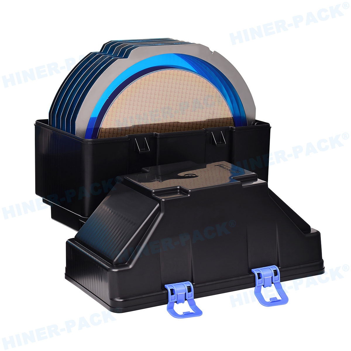
Wafer boxes for semiconductor processes serve as the first line of defense against contaminants like dust, moisture, and static electricity. In cleanroom environments, even microscopic particles can ruin entire batches of wafers, leading to substantial financial losses. These boxes are designed with materials such as high-purity plastics or composites that minimize outgassing and particulate generation. For instance, in advanced facilities, wafer boxes for semiconductor production ensure compatibility with automated handling systems, reducing human intervention and the risk of errors. This alignment with industry standards, including SEMI guidelines, underscores their vital role in maintaining wafer integrity from fabrication to assembly.
Types of Wafer Boxes and Their Applications
When selecting wafer boxes for semiconductor use, it’s essential to consider the specific application. Common varieties include standard wafer cassettes for intra-facility transport and specialized pods like FOUPs for 300mm wafers in front-end processes. These containers often feature anti-static properties and precise slot designs to prevent wafer slippage. In back-end operations, such as testing and packaging, wafer boxes for semiconductor logistics might include shock-absorbent features for safe shipping. Brands like Hiner-pack offer a range of options, from basic models to custom-designed solutions that cater to unique production lines. By matching the box type to your workflow, you can enhance throughput and reduce downtime.
Key Factors in Choosing the Right Wafer Box
Selecting the appropriate wafer boxes for semiconductor tasks involves evaluating several factors. Size compatibility is paramount—ensure the box matches your wafer diameter (e.g., 200mm or 300mm) and fits into existing equipment like load ports and robotics. Material selection also matters; polycarbonate or PEEK materials provide durability and low contamination rates. Additionally, consider the box’s weight, stackability, and compliance with international standards. For example, in high-volume fabs, opting for wafer boxes for semiconductor applications with RFID integration can streamline inventory tracking. Hiner-pack’s products often incorporate these features, emphasizing usability and long-term reliability in demanding environments.
Customization Options for Enhanced Performance
Not all semiconductor operations are identical, which is why customization plays a crucial role in wafer box selection. Custom wafer boxes for semiconductor use can be tailored to specific wafer thicknesses, handling mechanisms, or environmental conditions. This might include adding custom logos, color-coding for easy identification, or modifying latch mechanisms for quicker access. In one case study, a manufacturer reduced wafer breakage by 20% after switching to bespoke boxes designed with reinforced edges. Hiner-pack specializes in such tailored solutions, working closely with clients to develop wafer boxes for semiconductor processes that align with their unique needs, ultimately boosting efficiency and reducing waste.
Cost Considerations and Budgeting Tips
While quality is non-negotiable in semiconductor manufacturing, cost-effectiveness remains a key concern. The price of wafer boxes for semiconductor applications can vary based on material, customization, and volume. Generally, standard boxes are more affordable but may lack advanced features, whereas high-end models offer better protection at a premium. To optimize costs, consider bulk purchases or long-term partnerships with suppliers like Hiner-pack, which often provide volume discounts. Remember, investing in durable wafer boxes for semiconductor use can lead to lower replacement frequencies and fewer production halts, translating to better ROI over time. Always weigh initial expenses against potential savings from reduced contamination and improved yield.
Best Practices for Maintaining Wafer Boxes
Proper maintenance of wafer boxes for semiconductor operations is essential to extend their lifespan and ensure consistent performance. Start with regular cleaning protocols using approved solvents and lint-free wipes to remove residues. Inspect boxes for cracks, warping, or wear that could compromise wafer safety. Storage in controlled environments away from UV light and humidity helps prevent material degradation. Additionally, train staff on correct handling techniques to avoid mishaps. For instance, implementing a rotation system for wafer boxes in semiconductor fabs can distribute wear evenly. Hiner-pack’s guidelines often emphasize these practices, helping users maximize the utility of their containers while adhering to industry benchmarks.
The Importance of Supplier Selection
Choosing the right manufacturer for wafer boxes for semiconductor needs can make or break your production line. Look for suppliers with proven track records in the semiconductor sector, certifications like ISO 9001, and robust R&D capabilities. A reliable partner should offer technical support, warranty options, and flexibility for future upgrades. Hiner-pack, for example, has built a reputation for delivering high-quality wafer boxes for semiconductor applications, with a focus on innovation and customer service. By collaborating with such brands, you can access cutting-edge designs that keep pace with evolving industry trends, such as the shift toward larger wafers and greener materials.
In summary, wafer boxes for semiconductor manufacturing are indispensable tools that directly impact product quality and operational efficiency. From selection and customization to maintenance and cost management, each aspect requires careful attention to detail. As the semiconductor industry continues to evolve, staying informed about best practices and reliable suppliers like Hiner-pack will help you navigate challenges effectively. By implementing the solutions discussed, you can optimize your wafer handling processes and contribute to a smoother, more profitable production cycle.
Frequently Asked Questions (FAQs)
Q1: What are the primary functions of wafer boxes in the semiconductor industry?
A1: Wafer boxes for semiconductor manufacturing primarily protect wafers from physical damage, contamination, and environmental factors like humidity and static electricity. They ensure safe handling, storage, and transport during various stages of production, such as lithography and etching, while maintaining cleanroom standards.
Q2: How do I determine the right size and type of wafer box for my application?
A2: To choose the appropriate wafer boxes for semiconductor use, consider your wafer diameter (e.g., 150mm, 200mm, or 300mm), the specific process stage (e.g., fabrication or shipping), and compatibility with equipment like automated handlers. Consulting with suppliers like Hiner-pack can provide tailored recommendations based on your requirements.
Q3: What materials are commonly used in wafer boxes, and why are they important?
A3: Common materials for wafer boxes for semiconductor applications include high-purity polycarbonate, PEEK, and other static-dissipative plastics. These materials are chosen for their low particulate generation, chemical resistance, and durability, which help minimize contamination and extend the box’s lifespan in sensitive environments.
Q4: Can wafer boxes be customized, and what are the benefits?
A4: Yes, wafer boxes for semiconductor processes can be customized in terms of size, color, labeling, and features like integrated sensors or special latches. Customization improves efficiency by ensuring better fit with existing systems, enhancing traceability, and reducing handling errors, as seen in solutions from providers like Hiner-pack.
Q5: How often should wafer boxes be replaced or maintained?
A5: The maintenance schedule for wafer boxes in semiconductor settings depends on usage intensity and environmental conditions. Generally, inspect them monthly for signs of wear and clean them after each use. Replacement may be needed every 1-3 years, but high-quality boxes from brands like Hiner-pack can last longer with proper care, reducing overall costs.


