
In the semiconductor backend process, specifically during die sort, singulation, and final shipment, the margin for error is measured in microns. For manufacturers dealing with compound semiconductors (GaAs, InP), fragile MEMS structures, or high-value photonics, standard waffle packs often fail to provide adequate protection against mechanical shock during transit. This is where gel-based carrier technology becomes a critical infrastructure component.
As a procurement manager or process engineer, moving to a strategy of purchasing Bulk gel pak boxes is not merely an inventory decision; it is a yield preservation strategy. This article analyzes the technical specifications, material science, and supply chain considerations required to select the correct carrier systems for high-volume semiconductor operations.
The Physics of Gel Technology in Die Handling
To understand the value of these carriers, one must examine the material science governing the "gel" component. Unlike pressure-sensitive adhesives that leave residue, the elastomer material used in high-quality gel boxes relies on surface tension and cross-linked polymer chains to secure devices. This non-migrating material holds devices strictly through surface contact.
However, the challenge arises when devices become smaller (thinner than 150 microns) or extremely fragile. The holding force must be strong enough to prevent die migration during the high-G forces of shipping but weak enough to allow for die ejection without cracking the component. This balance is defined by the "Retention Level" (tackiness).
When you source Bulk gel pak boxes, you are primarily selecting between two mechanisms:
Standard Gel (Adhesive): The device is held by the intrinsic tack of the elastomer. Removal relies on the shear force of tweezers or a vacuum pickup tool overcoming the surface tension.
Vacuum Release (VR): The gel membrane is placed over a mesh. When a vacuum is applied to the underside of the tray, the gel conforms to the mesh shape, reducing the surface contact area by over 90%. This allows the device to be lifted with virtually zero force, critical for extremely fragile GaAs or thin-wafer applications.
Critical Specification 1: Determining the Correct Retention Level
One of the most common errors in bulk procurement is selecting a generic retention level. The tackiness must be inversely proportional to the device size and surface roughness. If the retention is too high for a small, smooth die, the vacuum tool may damage the device during pick-and-place operations. If it is too low for a heavy, rough-backed die, the device will shift during transport.
Common retention classifications typically range from x0 (Extra Low) to x8 (High).
x0 - x3 (Low Retention): Ideal for highly polished surfaces, such as optical lenses or beam splitters, where surface contact area is maximized naturally.
x4 - x5 (Medium Retention): The standard for most silicon dies and etched MEMS devices.
x6 - x8 (High Retention): Required for rougher ceramic substrates, PCBs, or heavy components that require significant holding force to counteract gravity and vibration.
Partnering with a specialized manufacturer like Hiner-pack allows engineers to sample different retention levels before committing to a volume order, ensuring the chosen specification matches the specific surface topography of the die.
Critical Specification 2: ESD Control and Material Composition
Electrostatic Discharge (ESD) is the silent killer in semiconductor logistics. When ordering Bulk gel pak boxes, the housing material is just as important as the gel itself. Standard polystyrene or polycarbonate boxes generate static charges that can attract particulate contamination or cause catastrophic failure in sensitive active devices.
Professional-grade carriers utilize specific conductive or static-dissipative materials:
Conductive Black (Surface Resistance < 10^5 ohms): This composite material allows for rapid charge decay. It is mandatory for most active semiconductor devices. The black color also provides contrast for automated optical inspection (AOI) systems.
Antistatic Clear (Surface Resistance 10^10 - 10^12 ohms): Useful when visual inspection through the box is required without opening it, though it offers less robust protection than conductive black.
Furthermore, the gel material itself must be electrically compatible. While the elastomer is naturally insulative, high-end variants incorporate proprietary additives to allow for a discharge path, preventing isolated charge buildup on the die surface.
Strategic Supply Chain: The Economic Case for Bulk Procurement
Procurement in the semiconductor industry is cyclical. During high-demand cycles, lead times for packaging consumables can stretch from weeks to months. Moving to a strategy of ordering Bulk gel pak boxes mitigates these risks.
Cost Analysis per Unit
The unit cost of a single Vacuum Release tray can be significant due to the complexity of manufacturing the mesh-gel interface. However, volume purchasing often reduces costs by 20-30% compared to spot-buying. This reduction is driven by manufacturing efficiencies—setting up the extrusion and curing lines for the gel material constitutes a major portion of the operational expense. Long production runs amortize this cost.
Inventory Consistency
A hidden advantage of bulk orders is lot consistency. Gel tackiness can vary slightly between manufacturing batches due to cure times and ambient humidity during production. By purchasing a year's supply in a single lot, process engineers guarantee a consistent release force for their pick-and-place robots, reducing the need for constant equipment recalibration.
Applications in Emerging Technologies
The demand for advanced packaging solutions is being driven by specific industry verticals that cannot utilize standard tape-and-reel or waffle packs.
Photonics and Optoelectronics
Laser diodes and optical filters have surfaces that cannot be touched or scratched. Even the slightest abrasion degrades optical performance. Gel technology suspends the device, ensuring the active optical facet never touches a hard surface. Suppliers like Hiner-pack have developed specialized cleaning protocols to ensure their boxes meet the low-outgassing requirements essential for optics.
3D-IC and Thinned Wafers
As wafers are ground down to 50 or 100 microns for 3D stacking, they become incredibly brittle. Vacuum Release (VR) technology is the only viable method for handling these dies. The ability to "switch off" the holding force via vacuum allows the die to be removed without any bending stress.
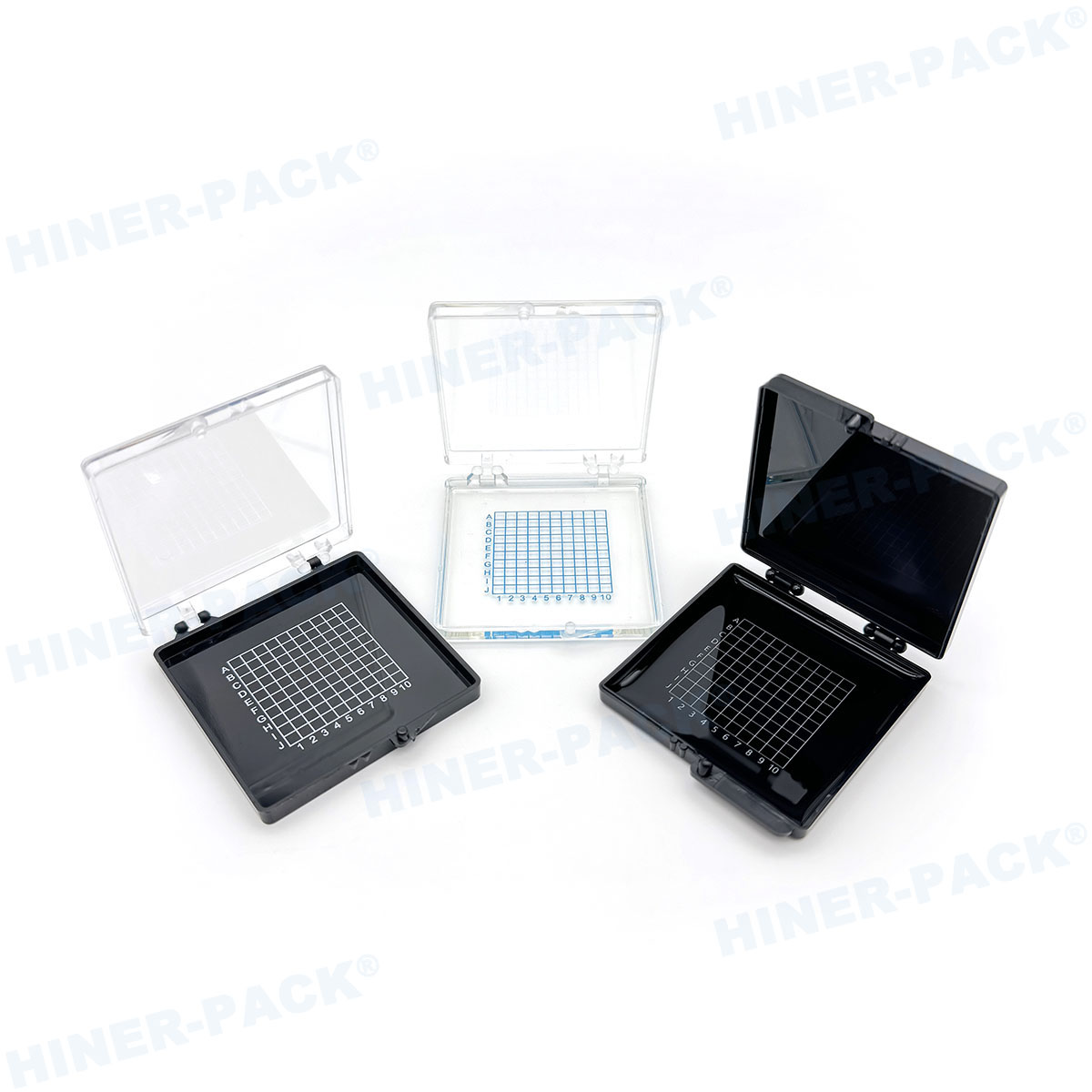
Visual Inspection and Grid Configurations
For manual handling or semi-automated lines, the visual layout of the box is vital. When sourcing Bulk gel pak boxes, buyers can specify printed grid patterns on the underside of the box or tray.
These grids (typically X/Y coordinates) enable operators to map defective dies or track specific bins within a single tray. For automated lines, fiducial marks can be printed to assist vision systems in aligning the pickup tool. This customization is usually only available or cost-effective when ordering in volume.
Storage and Shelf Life Considerations
Unlike standard plastics, gel boxes have a shelf life. The elastomer properties can evolve over time, particularly if exposed to extreme temperatures or UV light. When maintaining a bulk inventory:
Temperature Control: Store between 10°C and 30°C. Excessive heat can cause the gel to cure further, altering its retention properties.
UV Protection: Keep boxes in their original light-shielding packaging until use.
Timeframes: Most manufacturers guarantee performance for 2 years from the date of manufacture. A First-In-First-Out (FIFO) inventory system is essential.
Selecting the Right Partner
The manufacturing environment of the packaging supplier matters. If the gel box is manufactured in a facility with high particle counts, the box itself becomes a contamination source. A reputable supplier must manufacture and pack within a certified Cleanroom environment (Class 1000 or better).
Hiner-pack stands out in this sector by integrating advanced material research with strict contamination control protocols. Their ability to customize box dimensions, retention levels, and hinge designs makes them a preferred partner for foundries requiring reliable Bulk gel pak boxes that align with strict industry standards.
The selection of carrier systems is a technical engineering decision that directly impacts the final yield of semiconductor devices. By understanding the nuances of retention levels, ESD materials, and vacuum release mechanics, manufacturers can eliminate handling-induced defects. Transitioning to a bulk procurement model ensures supply chain resilience, cost efficiency, and process consistency.
Frequently Asked Questions (FAQ)
Q1: What is the primary difference between Standard Gel Boxes and Vacuum Release (VR) Trays?
A1: Standard Gel Boxes hold devices using only the surface tension of the gel; devices are removed using tweezers or force. Vacuum Release (VR) trays feature a mesh beneath the gel. When a vacuum is applied, the gel pulls down, reducing contact area by over 90%, allowing extremely fragile or thinned devices to be lifted off with zero force.
Q2: How do I determine the correct retention level for my devices?
A2: Retention level depends on device weight, surface roughness, and size. Heavier or rougher devices (like ceramics) require High retention (x6-x8). Small, smooth, or polished devices (like bare silicon or optics) require Low retention (x0-x3). Ordering Bulk gel pak boxes with the wrong retention can lead to die fly-off (too low) or difficulty in removal (too high).
Q3: Can Gel Pak boxes be cleaned and reused?
A3: While it is technically possible to clean the gel surface with compatible tape (like Scotch 810) to remove loose particles, it is generally not recommended for high-reliability semiconductor applications. Reuse increases the risk of cross-contamination and the gel's tackiness can degrade over time. For critical applications, single-use is best practice.
Q4: What is the typical temperature range for these boxes during shipping?
A4: Most standard gel boxes are designed to withstand temperatures ranging from -40°C to +60°C without losing their holding properties. However, for processes requiring high-temperature baking or cryogenic freezing, specialized high-temp or low-temp compatible box materials must be requested specifically from suppliers like Hiner-pack.
Q5: Why is "Conductive Black" preferred over clear boxes for most IC applications?
A5: Conductive Black materials provide a grounded path for electrostatic discharge, preventing static buildup that could destroy sensitive internal circuitry of the die. Clear boxes are usually insulating or only anti-static (dissipative) and are better suited for passive mechanical parts or optics where ESD is less of a concern.


