
Semiconductor assembly and test facilities depend on standardized carriers. A jedec tray (per JEDEC Standard No. 95) provides cavity arrays for IC shipping, baking, and automated pick-and-place. However, not all trays labeled "JEDEC" perform equally under thermal stress or high-speed handling. Hiner-pack has supplied over 8 million injection-molded trays to OSATs (Outsourced Semiconductor Assembly and Test) worldwide. This guide details nine verifiable parameters for procurement and process engineers.
1. JEDEC Tray Family Matrix: Matching Cavity Array to IC Package
The jedec tray specification defines outer dimensions and cavity layouts. Common families:
Type I: 322mm × 135mm – for QFP, QFN, BGA up to 27×27mm.
Type II: 322mm × 160mm – wider pitch for 35×35mm packages.
Type III: 322mm × 210mm – high-density arrays for DFN, SON.
Type IV: 340mm × 250mm – emerging for fan-out wafer-level packages (FOWLP).
Each family specifies cavity pitch, depth, and corner radii. Mismatched trays cause jams in magazine loaders. Always request the exact JEDEC outline drawing (MO-###) from your supplier.
2. Dimensional Tolerances: Critical for Automation Compatibility
Even within a standard jedec tray size, tolerances determine success. Verify three measurements:
Overall length/width: ±0.2mm max. Deviations cause misfeeds in stack magazines.
Cavity pocket depth: ±0.05mm for packages ≤1.2mm thickness. Excess depth allows IC tilting.
Corner radius: R1.0mm to R2.5mm per JEDEC. Sharp corners generate particles.
Hiner-pack uses coordinate measuring machines (CMM) with 1.2μm resolution. We provide a dimensional report with each batch.
3. Material Science: Conductive, Dissipative, and High-Temperature Grades
A jedec tray must control electrostatic discharge (ESD) and survive thermal cycles. Common materials:
Polystyrene (PS) with carbon filler: Surface resistivity 10⁵–10⁹ Ω/sq. Max 70°C, for ambient shipping.
Polycarbonate (PC): Withstands 120°C baking. Resistivity 10⁶–10¹⁰ Ω/sq.
Polyetherimide (PEI) / Ultem: Continuous use to 180°C. For solder reflow processes.
PEEK: 260°C resistance for lead-free soldering. Higher cost.
Hiner-pack recommends conductive PC for bake-and-ship cycles. We offer custom blends to meet specific surface resistivity (10⁴ to 10¹¹ Ω/sq).
4. Warpage Control Under Thermal and Humidity Stress
A jedec tray specification assumes flatness ≤0.3mm over full length. Real-world conditions cause warpage:
After 125°C baking: PC trays may warp 0.5–0.8mm if not annealed.
After humidity absorption (85°C/85% RH): Nylon-based trays swell, changing cavity pitch.
Solution: Request warpage data per IPC/JEDEC J-STD-020. Hiner-pack pre-conditions trays (bake + humidity) and measures flatness on a granite plate. Our trays maintain ≤0.25mm warpage after 48 hours at 125°C.
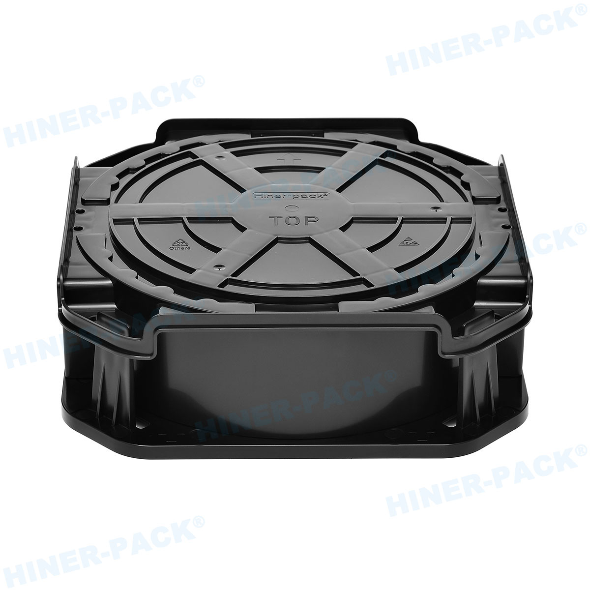
5. Stacking and Interlocking Features for Automatic Handling
Stacked trays feed pick-and-place machines. Poor stacking ribs cause jams. Verify on any jedec tray:
Stacking ribs height: 2.0mm ±0.1mm to prevent IC-to-lid contact.
Interlocking pins and sockets: Conical design with 0.2mm clearance.
Alignment corners: Chamfered or notched for optical sensors.
Hiner-pack's molds include anti-backlash stacking pins. A recent customer test showed 50,000 tray cycles without misfeed.
6. Cleanliness and Particle Generation Standards
Semiconductor contamination control extends to shipping trays. Requirements for a jedec tray:
Ionic contamination: ≤0.1 µg/cm² NaCl equivalent per IEST-STD-CC1246.
Outgassing: No silicone-based mold release. FDA-grade lubricants only.
Particle shedding: ≤10 particles ≥0.5µm per tray after 10 minutes vibration.
IC shipping trays from Hiner-pack are molded in ISO Class 7 cleanrooms (Class 10,000) with ionized air rinsing. We provide a Certificate of Analysis (CoA) for each lot.
7. Common Industry Pain Points and Corrective Actions
OSAT engineers report recurring issues with jedec tray products from low-cost suppliers. Here are three and their fixes:
Problem: ICs stick in cavities after baking. Root cause: Cavity draft angle <1°. Fix: Specify 1.5° to 2° draft and polished cavity surfaces (SPI-A2 finish).
Problem: Trays crack at stacking corners during autoclave. Root cause: Sharp radii stress concentration. Fix: Increase corner radius to R2.0mm and use PC with 20% glass fiber.
Problem: Tray dimensions shrink after multiple reflow cycles. Root cause: Using PEI below Tg. Fix: Upgrade to PEEK or limit tray exposure to ≤5 reflow cycles.
Hiner-pack's engineering team performs failure analysis on returned trays at no charge, delivering a root cause report within 10 days.
8. Automation Compatibility: Tray-to-Equipment Interface
Beyond dimensions, a jedec tray must interface with specific handlers. Verify:
Magazine pitch compatibility: Standard magazines accept trays every 8mm or 12mm. Tray thickness must be 4.0mm ±0.1mm.
Barcode pocket location: JEDEC specifies a 25mm × 10mm area on the tray edge for 2D data matrix codes.
Vacuum pickup zones: Smooth bottom surface with no ejector pin marks in the cavity area.
Hiner-pack provides 3D STEP files of each tray for virtual validation in your equipment software (Fujisu, Yamaha, Datacon).

9. Why Hiner-pack Leads in JEDEC-Compliant Tray Manufacturing
With 22 injection molding presses (80 to 550 tons) and in-house tooling, Hiner-pack produces jedec tray products that exceed standard tolerances. Our advantages:
Tooling guarantee: All molds include replaceable cavity inserts, reducing requalification costs when IC dimensions change.
Material traceability: Lot numbers on every tray, linked to raw material certificates.
Rapid prototyping: 3D-printed sample trays in 5 days for fitment testing.
Global logistics: Warehouses in Taiwan, China, Malaysia, Mexico, and Germany with consignment stock programs.
Hiner-pack's trays are used by ASE, Amkor, and JCET for automotive, medical, and high-reliability ICs.
Frequently Asked Questions (FAQ)
Q1: What is the difference between a JEDEC tray and a matrix
tray?
A1: JEDEC trays follow specific dimensional standards (JESD95)
for outer size and cavity pitch, ensuring interoperability. "Matrix tray" is a
generic term; many matrix trays are JEDEC-compliant, but some are not. Always
verify with the supplier's datasheet.
Q2: Can a JEDEC tray be used for ICs with exposed die or wire
bonds?
A2: No. Standard rigid cavities can damage wire bonds or die
surfaces. For sensitive devices, Hiner-pack offers custom overmolded trays with
soft silicone gel inserts or foam liners.
Q3: How do I test if a JEDEC tray meets moisture sensitivity level
(MSL) requirements?
A3: Request MSL testing per J-STD-020. The tray
material must absorb <0.2% moisture after 168 hours at 85°C/85% RH.
Hiner-pack provides MSL-1 certified trays for PC and PEI materials, with test
reports.
Q4: What lead time for a custom JEDEC tray with a new cavity
pattern?
A4: For a new injection mold: 6–8 weeks (including mold
flow analysis and first article inspection). Hiner-pack offers 4-week expedited
service using aluminum prototype molds for up to 5,000 trays.
Q5: Are JEDEC trays recyclable after use?
A5: Yes. PS,
PC, and PEI trays are mechanically recyclable. Hiner-pack operates a take-back
program: we grind used trays into regrind and recompound into non-critical
shipping trays, reducing landfill waste by 90%.
Request a JEDEC Tray Sample Kit and Engineering Consultation
Selecting the correct jedec tray for your IC package reduces handling damage and improves automation yield. Hiner-pack provides free sample trays (up to 50 pieces) for fitment testing on your pick-and-place equipment. We also offer dimensional inspection reports, warpage data, and material certificates.
Contact Hiner-pack’s semiconductor
division:
Website: https://www.waferboxes.com/
Email:
rainbowzhu@hiner-pack.com
Phone:+86 755 2322 9236
Send your IC package dimensions (body size, thickness, pin count), annual volume, and handling equipment model. Hiner-pack will reply with a CAD drawing, pricing, and a 3D-printed sample within 5 business days.


