
Yield loss is the enemy of every semiconductor fabrication plant. After weeks of processing, lithography, and etching, the physical movement of silicon between facilities represents one of the highest risk points in the supply chain. While much of the industry buzz focuses on 300mm automation, the 200mm (8-inch) sector remains the backbone of power electronics, MEMS, and IoT sensors.
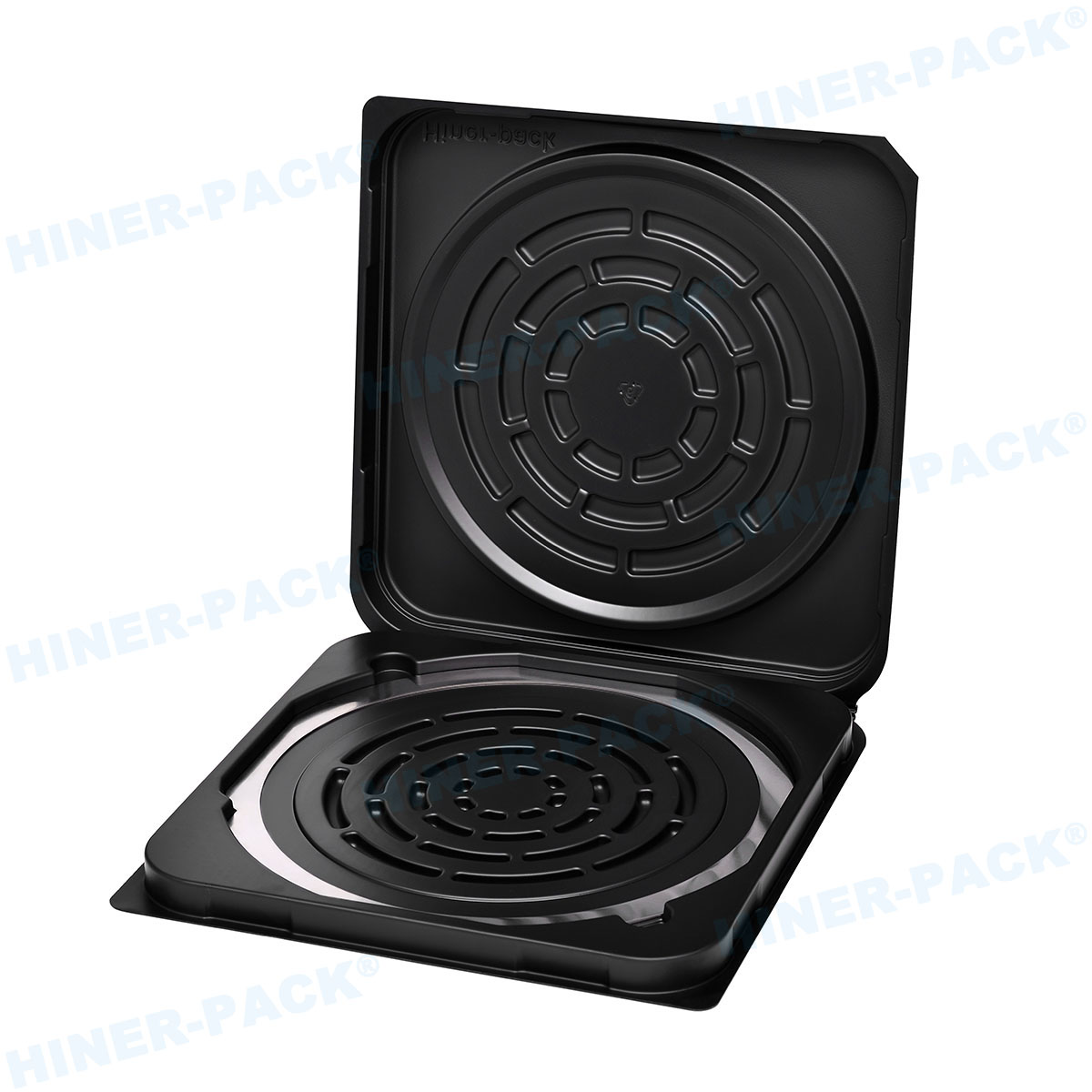
This makes the humble 8-inch Wafer Jar a critical component in the manufacturing process. It is not merely a plastic container; it is the primary barrier between a finished wafer and the chaotic environment of a shipping truck or cargo hold.
Selecting the right container involves understanding material properties, ESD (Electrostatic Discharge) safety, and mechanical fit. At Hiner-pack, we see firsthand how the right packaging choice impacts the bottom line for fabs and test houses.
Why the 8-inch Wafer Jar Remains Critical in Modern Fabs
There was a time when analysts predicted the end of the 200mm wafer. They were wrong. The demand for analog chips, display drivers, and automotive microcontrollers has breathed new life into older fabrication nodes. Consequently, the logistics infrastructure for these wafers must be maintained and improved.
Unlike 300mm FOUPs (Front Opening Unified Pods) which are fully automated and rarely leave the fab environment, the 8-inch Wafer Jar is often used for inter-facility transport. Wafers might be processed in one location, sent to a foundry for back-grinding, and then shipped to an assembly house for packaging.
During these transitions, the wafers are exposed to vibration, temperature changes, and potential human error. A standard shipping box cannot handle these variables. The jar provides a rigid, clean micro-environment that maintains the integrity of the silicon structure.
Material Matters: Selecting the Right Plastic for Your 8-inch Wafer Jar
Not all plastics are created equal. When sourcing a jar, the base material dictates its performance regarding outgassing and static protection.
Polypropylene (PP) is a common choice for standard applications. It offers a good balance of impact resistance and cost. However, for highly sensitive devices, standard PP might hold a static charge that attracts particles.
This is where Carbon Powder or Carbon Fiber filled polymers come into play. These materials create a conductive or static-dissipative path. If an operator touches the jar, the static charge bleeds off slowly rather than snapping into the wafer.
High-end applications often require PFA (Perfluoroalkoxy) or specialized Polycarbonate blends. These materials offer superior chemical resistance and low outgassing properties. Outgassing occurs when the plastic releases volatile organic compounds (VOCs) over time. If these VOCs condense on the wafer surface, they can cause defects in sensitive layers.
Hiner-pack’s Approach to Wafer Safety and Design
At Hiner-pack, we understand that the fit of the wafer inside the container is paramount. If the tolerance is too loose, the wafers will rattle against the sidewalls during transit, leading to edge chipping or particle generation.
Our design philosophy for the 8-inch Wafer Jar centers on "secure suspension." The internal slots or cassette mechanism must hold the wafers firmly by the edges without exerting stress that could cause warpage.
We also focus heavily on the closure mechanism. A jar that pops open if dropped is a catastrophic failure. The threading or snap-lock system on Hiner-pack containers is engineered to withstand significant G-forces. We test for drop resilience to ensure that the seal remains airtight even under rough handling conditions.
Controlling Contamination and Particles
Particle generation is a major concern when wafers slide into and out of a container. This is known as "friction abrasion."
A high-quality 8-inch Wafer Jar minimizes contact surface area. The design should ensure that the wafer only touches the container at the very edge of the exclusion zone (usually the outer 3mm).
Furthermore, the jar itself must be manufactured in a cleanroom environment. If the container arrives at the fab carrying dust from the molding factory, it defeats the purpose.
Hiner-pack ensures that our packaging products are molded, assembled, and packed in controlled cleanroom environments. This reduces the burden on the customer to perform aggressive pre-cleaning before use.
Handling and Shipping Protocols for the 8-inch Wafer Jar
Owning the right jar is only half the battle. How your logistics team packs the jar determines the success of the shipment.
Standard protocol usually involves placing the wafers into the jar, securing the lid, and then double-bagging the entire unit. The inner bag is often a moisture barrier bag (MBB), vacuum-sealed to prevent humidity ingress.
The 8-inch Wafer Jar should then be placed in a secondary box with foam cushioning. The foam density matters. If the foam is too soft, the jar bottoms out during a drop. If it is too hard, the shock transfers directly to the silicon.
We recommend using shock indicators on the outer packaging. These small labels turn red if the package has been dropped from a specific height, alerting the receiving team to inspect for breakage immediately.
The Role of Gaskets and Seals
For long-term storage or sea freight, air exchange is a problem. Salt air or humid environments can corrode metalized layers on a wafer.
Many standard jars rely on the plastic-to-plastic fit for sealing. While this is sufficient for short trips, it is not airtight.
Premium versions of the 8-inch Wafer Jar may include an elastomeric gasket in the lid. This creates a hermetic seal. However, one must be careful with gasket materials. Like the jar body, the gasket must not outgas. Silicone is common but can migrate; therefore, specialized fluoroelastomers are often preferred for high-purity applications.
Comparing Single Wafer Shippers vs. Multi-Wafer Canisters
There are two main categories of transport containers: single wafer shippers and coin-stack/cassette style jars.
Single wafer shippers are expensive per unit of silicon but offer the highest protection. They are typically used for mask reticles or extremely high-value engineering samples.
For volume production, the multi-wafer 8-inch Wafer Jar is the standard. These typically hold 25 wafers. The challenge with these is the "domino effect." If a jar is crushed, you lose 25 wafers instantly.
This risk underscores the need for high-impact resistant materials. Hiner-pack designs our multi-wafer solutions with reinforced ribs on the exterior. These ribs act as crumple zones, absorbing impact energy before it reaches the wafer stack.
Reuse and Sustainability in Semiconductor Packaging
The semiconductor industry produces a significant amount of plastic waste. Can these jars be reused?
The answer is yes, but with strict caveats. A reused 8-inch Wafer Jar must undergo a rigorous cleaning process. This usually involves an ultrasonic wash in deionized water and a surfactant, followed by a bake-out to remove moisture.
However, repeated washing can degrade the ESD coating on some plastics. It is vital to test the surface resistivity of the jar after a certain number of cycles.
Hiner-pack supports sustainability by using recyclable polymers where possible. We work with clients to determine the lifecycle of our products, ensuring that when a jar reaches the end of its usable life, it can be processed responsibly.
The Cost of Quality: Why Cheap Jars Are Expensive
Procurement departments often look at the unit price of a plastic jar and opt for the cheapest option. In the context of semiconductor manufacturing, this is a dangerous calculation.
An 8-inch processed wafer can be worth anywhere from $500 to over $5,000, depending on the complexity of the circuitry. A jar holding 25 of these carries inventory worth tens of thousands of dollars.
Saving a few dollars on a generic 8-inch Wafer Jar that lacks proper ESD protection or structural integrity is a massive financial risk. If a generic jar generates particles that lower yield by just 1%, the financial loss far exceeds the cost of premium packaging.
Hiner-pack positions our products as yield-insurance. We provide the documentation, the material traceability, and the design validation that process engineers require to sleep soundly.
The 200mm ecosystem is robust and growing. As chips become more integral to automotive and industrial applications, the physical safety of these components during transit becomes a priority.
Choosing the right 8-inch Wafer Jar requires a balance of material science, mechanical engineering, and logistical planning. It is about protecting the investment made in every layer of silicon.
Whether you are shipping raw substrates or fully patterned wafers, Hiner-pack offers the expertise and product reliability needed to ensure your products arrive ready for the next step in the process. Don't let the last mile of the journey be the weak link in your supply chain.
Frequently Asked Questions (FAQ)
Q1: What is the difference between a PFA and a PP 8-inch Wafer Jar?
A1: PFA (Perfluoroalkoxy) offers higher chemical resistance, higher temperature tolerance, and lower outgassing compared to PP (Polypropylene). PFA is typically used for high-purity applications where contamination must be near zero, while PP is used for standard transport due to its cost-effectiveness and durability.
Q2: How do I clean an 8-inch Wafer Jar for reuse?
A2: Cleaning typically involves an ultrasonic bath using Deionized (DI) water and a mild, non-ionic surfactant. It is crucial to avoid abrasive scrubbing which can scratch the plastic and generate particles. After washing, the jar should be dried in a cleanroom oven to remove all moisture. Always verify particle counts before reusing.
Q3: Can Hiner-pack jars protect against Electrostatic Discharge (ESD)?
A3: Yes, we offer specific models manufactured from conductive or static-dissipative materials. These materials allow static charges to bleed off safely, preventing sudden sparks that could damage sensitive micro-circuitry on the wafers.
Q4: How many wafers does a standard 8-inch Wafer Jar hold?
A4: The industry standard capacity is usually 25 wafers per jar. However, depending on the thickness of the wafers and the specific design of the cassette or "coin stack" insert, some configurations may hold fewer wafers to allow for spacers or protective interleaf paper.
Q5: What is the maximum temperature an 8-inch Wafer Jar can withstand?
A5: This depends entirely on the material. Standard Polypropylene jars are generally safe up to around 60°C - 80°C. Polycarbonate can handle higher temperatures, while high-grade PFA jars can withstand temperatures exceeding 200°C, making them suitable for specific bake-out processes, though transport usually occurs at ambient temperatures. Always check the specific datasheet for the jar you are using.


