
In semiconductor manufacturing, the journey of a silicon substrate doesn't end after the cleanroom processing steps are complete. The logistics of moving these valuable discs from one facility to another, or storing them for future use, is a critical operational phase. For high-volume handling of 150mm substrates, the 6-inch Wafer Jar remains the backbone of bulk semiconductor packaging.
At Hiner-pack, we see packaging not just as a container, but as the final line of defense for your yield. A single particle or a micro-crack during storage can render a batch of chips useless.
While 300mm fabs rely on automated FOUPs, the 150mm (6-inch) market—dominated by power electronics, LEDs, and MEMS—relies heavily on robust, manual, or semi-automated jar solutions. This article examines the technical necessity of these containers and how to ensure they serve your production line effectively.
The Engineering Necessity of the 6-inch Wafer Jar
Why do fabs still use jars instead of just shipping in process cassettes? The answer lies in contamination control and shock absorption.
A process cassette is designed for fluid flow and robotic handling. It is open to the air. If you transport wafers across a facility or ship them overseas in a standard cassette, they are exposed to particulates and humidity.
The 6-inch Wafer Jar is designed to create a sealed micro-environment. When the lid is screwed on or clamped shut, it creates a barrier against the outside world.
This isolation is vital. During air freight, pressure changes can force air in and out of imperfectly sealed containers. A high-quality jar minimizes this "breathing" effect, keeping the internal nitrogen or cleanroom air stable.
Furthermore, jars are designed for density. Shipping 25 wafers in single shippers creates a massive volume footprint. A jar consolidates this into a compact cylinder, drastically reducing freight costs per wafer.
Material Science: Choosing the Right Polymer
Not all plastic is created equal. The material composition of your storage container interacts directly with your substrate.
Most standard jars are manufactured from high-purity Polypropylene (PP). This material is chosen for its chemical resistance and relatively low cost. It is tough and can survive drops.
However, for sensitive applications, outgassing is a concern. Standard plastics can release volatile organic compounds (VOCs) over time. These VOCs can deposit on the wafer surface, creating a haze that interferes with wire bonding or further lithography.
Hiner-pack strictly controls the raw materials used in our manufacturing process. We look for low-outgassing polymers that do not migrate additives onto the silicon.
For extremely sensitive devices, manufacturers might opt for PFA or specialized Polycarbonate, though PP remains the industry workhorse for standard 6-inch logistics.
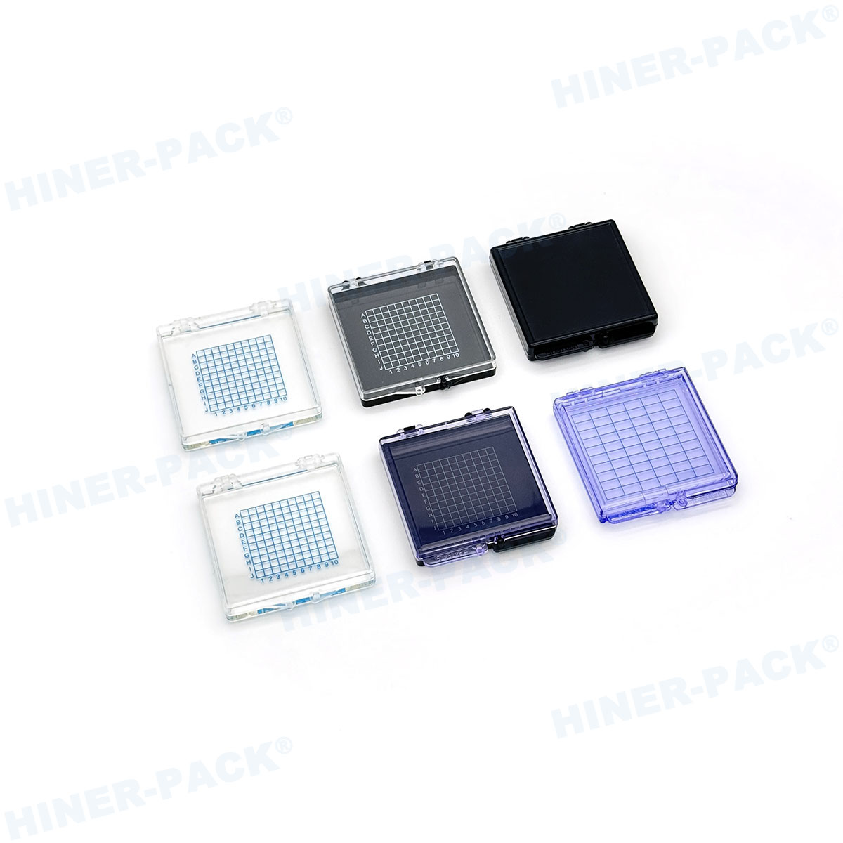
Managing Static with a Conductive 6-inch Wafer Jar
Static electricity is an invisible enemy. As wafers slide in and out of slots, friction generates charge. If this charge isn't dissipated, it can discharge through the micro-circuitry on the chip, causing latent defects.
This is where the difference between "natural" and "conductive/ESD" jars becomes apparent.
Natural PP jars are electrically insulating. They are fine for bare silicon or mechanical grade wafers. However, for processed wafers with active circuitry, you need an ESD-safe solution.
Conductive jars usually contain carbon powder or carbon fibers mixed into the plastic matrix. This turns the container into a Faraday cage of sorts.
When a charged operator touches the jar, the current flows around the container rather than through the wafers. At Hiner-pack, we recommend testing surface resistivity regularly to ensure the ESD properties haven't degraded over time.
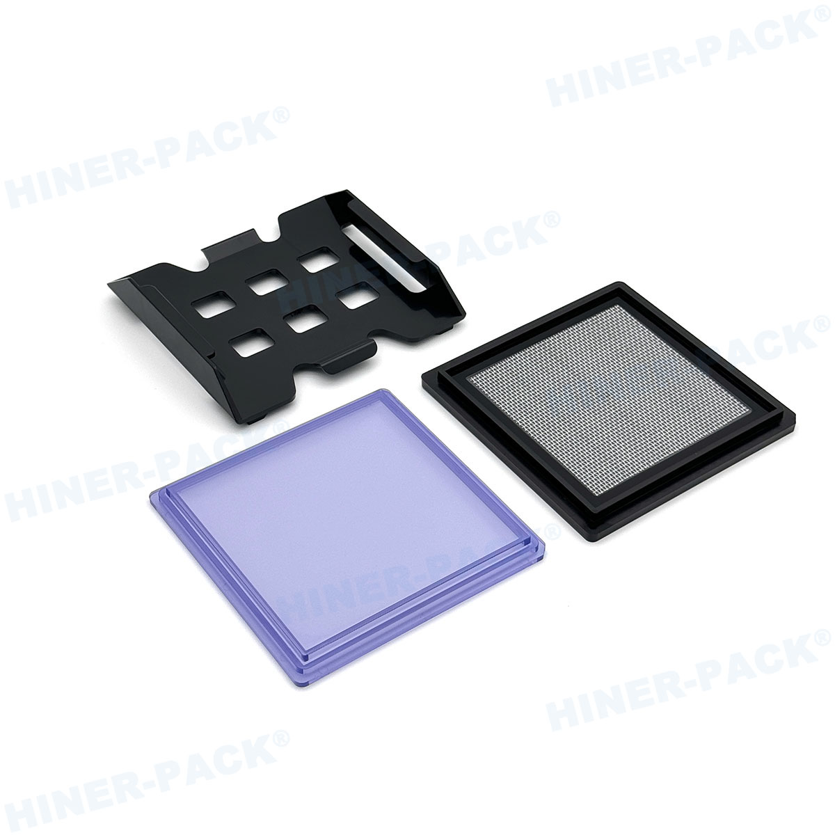
Internal Cushioning: The Art of the Stack
A jar alone is rarely enough. If you place 25 wafers in a jar with loose spacing, they will rattle. That movement generates particles.
To secure the load, the industry uses a combination of foam discs and separators.
Typically, a stack starts with a cushion of cleanroom-grade foam at the bottom. Wafers are then stacked.
If the wafers are fully processed, they cannot touch each other. Interleaf circles made of Tyvek or carbon-loaded paper are placed between them. These separators prevent scratches on the active face.
Once the stack reaches the top, more foam is added to fill the void. The lid of the 6-inch Wafer Jar then compresses this foam "spring."
This compression is critical. It turns 25 individual brittle discs into a single, solid block. A solid block withstands shock much better than loose components.
Cleaning and Reusability Protocols
One of the financial benefits of using jars is reusability. Unlike single-use packing materials, a high-quality jar can be used for years.
However, reuse introduces the risk of cross-contamination. A jar that carried copper-seeded wafers cannot be used later for virgin silicon without rigorous cleaning.
The cleaning process typically involves ultrasonic baths with de-ionized (DI) water and specific surfactants.
The design of the jar matters here. Sharp corners or deep, unpolished grooves can trap particles and chemical residue. Hiner-pack focuses on mold designs with smooth internal transitions to facilitate easy draining and drying.
After washing, the jars must be dried in a cleanroom environment. Water spots are a major source of contamination.
Fab managers should implement a tracking system. Mark the jars to indicate what material they previously held. Segregating your jar fleet prevents "killer defects" from migrating between process lines.
Logistics Strategy for the 6-inch Wafer Jar
Once packed, the jar moves to the shipping dock. But you cannot simply toss a jar into a cardboard box.
The standard procedure involves a "box-in-box" approach. The jar is first placed inside a moisture barrier bag (MBB). This bag is often vacuum-sealed.
Vacuum sealing serves two purposes. First, it locks the lid in place. Second, it prevents humidity ingress. Humidity can cause oxidation on copper pads or aluminum interconnects.
This bagged jar is then placed in a slot-fitted foam box. The foam box is then placed in a corrugated cardboard carton.
This multi-layer approach ensures that even if the outer box is pierced or crushed, the 6-inch Wafer Jar inside remains intact.
For international shipping, always include a humidity indicator card inside the vacuum bag. This tells the receiving engineer if the seal was compromised during transit.
Addressing Warped and Thinned Wafers
The semiconductor industry is pushing boundaries with TAIKO grinding and ultra-thin substrates. Standard jars can sometimes be problematic for these.
A standard 6-inch wafer is roughly 675 microns thick. Thinned wafers can be 100 microns or less.
If you stack 25 thinned wafers, the stack height is significantly lower. The standard foam fillers might not provide enough compression.
In these cases, spacer rings or extra foam fillers are required. Furthermore, thinned wafers are flexible. If the foam compresses them unevenly, they can warp or crack.
Operators handling thinned wafers in jars must be extremely gentle. The suction from removing a wafer from a tight stack can sometimes break a thin substrate.
Hiner-pack works with clients to customize the internal spacing and cushioning materials to accommodate these non-standard thicknesses.
Storage Economics: Jar vs. Cassette
Space is expensive in a cleanroom. Storing wafers in open cassettes takes up significant shelf space and requires constant airflow management to keep dust away.
Jars allow for high-density vertical storage. Because they are sealed, they can be stored on standard shelving outside the primary cleanroom aisles, provided the temperature is controlled.
This reduces the load on the high-class cleanroom areas. You can archive batches of test wafers or slow-moving inventory in jars without worrying about degradation.
From a cost perspective, a jar is a fraction of the price of a PFA process cassette. Using cassettes for long-term storage is a waste of capital assets. Moving inventory into Hiner-pack jars frees up your cassettes for active production lots.
The Role of the 6-inch Wafer Jar in Emerging Markets
While 12-inch silicon dominates high-logic chips, the 6-inch market is exploding with Silicon Carbide (SiC) and Gallium Nitride (GaN).
These wide-bandgap materials are expensive. A single 6-inch SiC wafer can cost thousands of dollars.
When the cargo value is this high, the container cost is negligible, but the container performance is paramount.
SiC is brittle and hard. It reacts differently to shock than silicon. The jar used for SiC often requires stiffer sidewalls to prevent any flexing that could snap the crystal.
Furthermore, these compound semiconductors are often used in high-voltage applications. Any ionic contamination from the plastic jar can be catastrophic. This drives the demand for ultra-pure, certified raw materials in jar production.
Common Operational Mistakes
We often see operators making simple errors that compromise the pack.
One common mistake is over-tightening the lid. While a tight seal is good, over-tightening can strip the threads. Once threads are damaged, plastic shavings are generated directly above the wafers.
Another error is mixing foam types. Using non-cleanroom foam (like standard pink packing foam) inside the jar is a disaster. It sheds particles rapidly. Always use cleanroom-certified polyethylene or polyurethane foam.
Finally, failing to burp the jar. If you seal a jar in a cold room and move it to a hot truck, the pressure builds up. Conversely, sealing in a warm room and moving to a cold cargo hold creates a vacuum. Some advanced jars have breather valves, but for standard ones, temperature stability during packing is key.
The humble 6-inch Wafer Jar is more than just a plastic bucket. It is a precision-engineered tool that bridges the gap between manufacturing and application.
Whether you are handling legacy silicon, cutting-edge SiC, or fragile glass substrates, the integrity of your packaging determines the success of your delivery. By understanding the materials, the packing mechanics, and the logistics protocols, you can virtually eliminate shipping-related yield loss.
Hiner-pack remains committed to providing the semiconductor industry with robust, clean, and reliable packaging solutions. When you trust your wafers to our jars, you are ensuring that the hard work done in the fab translates to performance in the field.
Frequently Asked Questions (FAQ)
Q1: How many wafers can a standard 6-inch Wafer Jar hold?
A1: The industry standard capacity is 25 wafers per jar. However, this depends on the wafer thickness and the amount of spacing material (separators and foam) used. If you are shipping thinner wafers or require thick foam dividers, the capacity might be reduced to ensure a safe, snug fit.
Q2: Can Hiner-pack jars be used for automated loading systems?
A2: Most wafer jars are designed for manual or semi-manual loading. While some automated bulk transfers exist, jars generally do not have the precise registration slots found on FOUPs or process cassettes. They are primarily intended for storage and shipping rather than active track processing.
Q3: What is the best way to clean a 6-inch Wafer Jar for reuse?
A3: The best practice is to use an ultrasonic cleaning tank with a mild, residue-free surfactant followed by a thorough rinse with de-ionized (DI) water. The jars must be dried in a cleanroom environment, often using nitrogen blow-dryers or HEPA-filtered drying cabinets, to effectively prevent water spots and particle adhesion.
Q4: Do I need ESD-safe jars for all wafer types?
A4: No, not all wafers require ESD protection. If you are shipping raw, unpolished silicon ingots or wafers without active circuitry, standard natural polypropylene jars are sufficient. However, for processed wafers with metallic layers or active devices, ESD-safe (conductive or dissipative) jars are essential to prevent electrostatic discharge damage.
Q5: Is vacuum sealing necessary for shipping the 6-inch Wafer Jar?
A5: While not strictly mandatory for short distances, vacuum sealing the jar inside a moisture barrier bag is highly recommended for international or air freight. It prevents moisture ingress and adds a secondary layer of security that keeps the lid from vibrating loose due to air pressure changes in the cargo hold.


