
In semiconductor front-end and back-end manufacturing, the wafer hoop ring (often referred to as a wafer frame or wafer carrier ring) serves as the structural backbone for mounting wafers during dicing, die attach, wire bonding, and transport. A poorly specified hoop ring leads to wafer warpage, edge chipping, and misalignment in automated handling systems. Hiner-pack has supplied precision hoop rings for over 15 years to IDMs, OSATs, and wafer foundries, focusing on dimensional stability, electrostatic discharge (ESD) properties, and cleanroom compatibility. This article details the engineering parameters that separate a reliable hoop ring from a recurring source of yield loss.
1. Core Functions of a Wafer Hoop Ring in Semiconductor Workflow
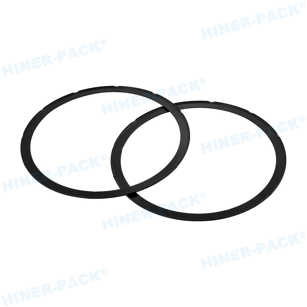
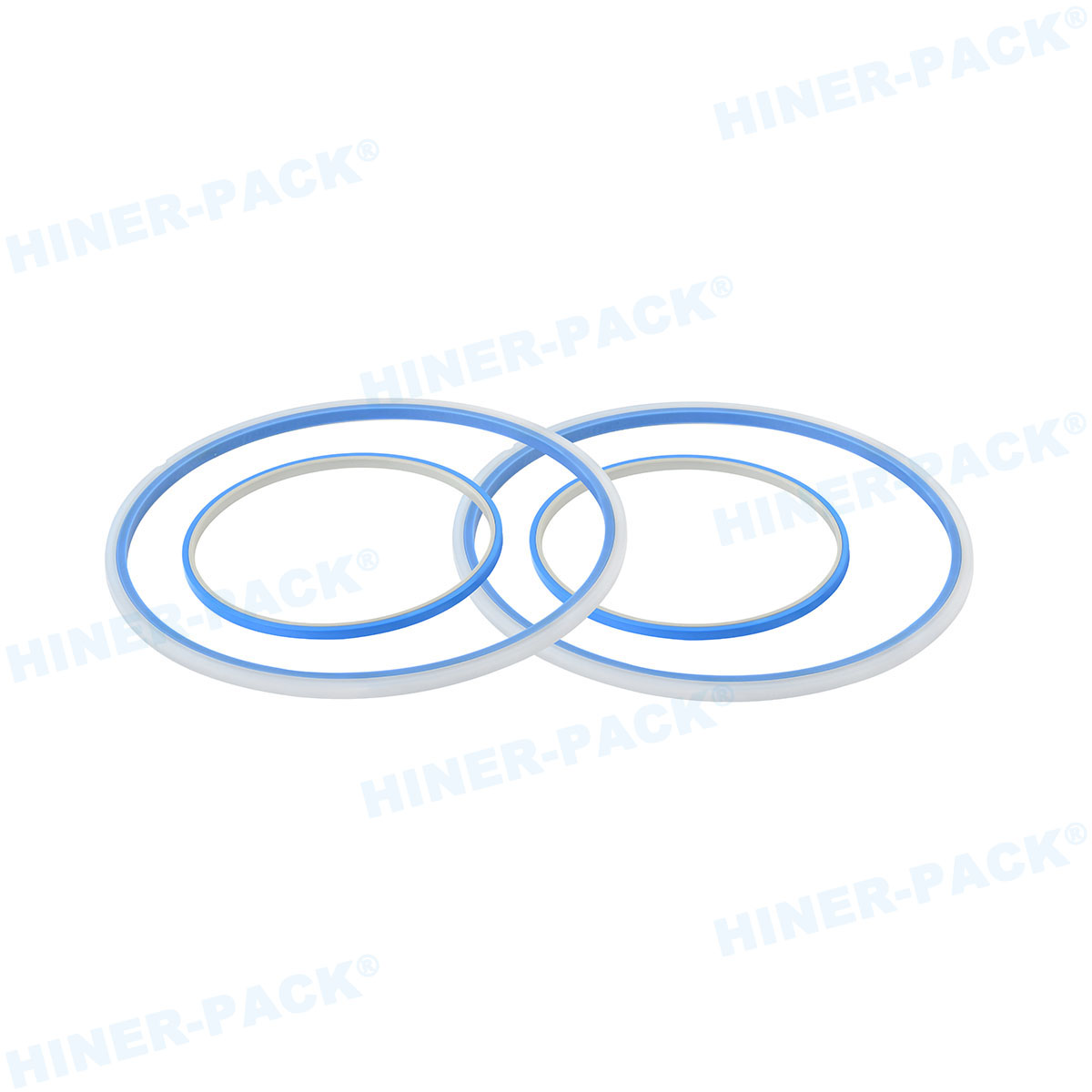
The wafer hoop ring is a rigid annular frame that holds a wafer (typically 200mm or 300mm) via an adhesive tape stretched across the ring. Its primary roles include:
Wafer dicing support: The ring holds the wafer steady on the dicing tape, preventing die shift during sawing.
Die transport and storage: After dicing, the ring remains as a frame for the diced wafer (wafer on a film frame), allowing pick-and-place equipment to access individual dies.
Interfacing with automated equipment: Hoop rings are designed to nest precisely into wafer expanders, die sorters, and die bonders (e.g., Datacon, ESEC, Shinkawa).
Cleanroom compatibility: Materials and surface finishes must minimize particle shedding, ionic contamination, and outgassing.
For high-volume manufacturing, the hoop ring must also withstand repeated thermal cycles (from -40°C storage to +85°C die attach) without warping or losing dimensional accuracy. Hiner-pack's hoop rings are validated to maintain flatness within 0.1 mm across the entire 300 mm diameter after 100 temperature cycles.
2. Material Selection: Stainless Steel vs. PEEK vs. Carbon Fiber
The choice of hoop ring material directly affects cost, durability, and process compatibility. Three options dominate the market:
Stainless steel (304 or 316): High stiffness, excellent dimensional stability, and good thermal conductivity. However, stainless steel is heavy (approx. 600g for a 300mm ring) and can cause wafer damage if dropped. Surface treatment (electropolishing or passivation) is mandatory to reduce particle generation. Best for high-mix, low-volume R&D lines.
PEEK (polyether ether ketone): Lightweight (approx. 150g for 300mm), chemically resistant, and inherently static-dissipative (surface resistivity 10⁶–10⁹ Ω/sq when modified). PEEK rings absorb less moisture than other polymers, maintaining flatness in humid environments. Hiner-pack uses medical-grade PEEK with laser marking for traceability. Preferred for high-volume automated die bonding where ring weight affects indexing speed.
Carbon fiber composite: Extremely high stiffness-to-weight ratio, near-zero thermal expansion. Used for ultra-thin wafer handling (<100µm thickness) where any ring deflection transfers to wafer breakage. However, carbon fiber is expensive (3-5x PEEK) and can generate conductive dust if edges are not sealed. Limited to advanced packaging applications (e.g., fan-out wafer-level packaging).
For most OSATs and IDMs, PEEK offers the best balance. Hiner-pack provides a wafer shipping and handling product line including PEEK hoop rings with embedded RFID for automated tracking.
3. Dimensional Specifications and Flatness Requirements
A wafer hoop ring must conform to SEMI standards (e.g., SEMI G88-0303 for 200mm film frames, SEMI G94-0206 for 300mm) to ensure compatibility with industry equipment. Critical parameters include:
Outer diameter (OD): 200mm rings have OD = 230.0 ±0.2 mm; 300mm rings have OD = 360.0 ±0.3 mm. Deviation prevents proper seating in ring holders.
Inner diameter (ID): The wafer pocket diameter must be 0.5–1.0 mm larger than the wafer diameter to allow thermal expansion without edge contact. For a 300 mm wafer, ID = 301.0 ±0.1 mm.
Thickness: Typically 1.5–2.0 mm for stainless steel, 2.5–3.0 mm for PEEK to achieve equivalent rigidity. Thickness variation across the ring must be <0.05 mm to prevent rocking on the vacuum chuck.
Flatness (total indicated runout): Maximum warp under its own weight: ≤0.15 mm for stainless steel, ≤0.20 mm for PEEK. Measured on a granite surface plate with a dial indicator.
Corner radii and edge break: All edges must be deburred and have a radius of 0.2–0.5 mm to avoid cutting the mounting tape or damaging operator gloves.
Hiner-pack inspects every hoop ring using a coordinate measuring machine (CMM) and provides a certificate of conformance with each shipment. Rejection rate for out-of-tolerance rings is below 0.3%.
4. Surface Finish and Cleanroom Compatibility
Particle generation from hoop rings is a major source of wafer defects (killer particles >0.3µm). The surface finish must balance low friction (to avoid tape abrasion) with low particle shedding.
For stainless steel: Mechanical polishing to Ra ≤0.4 µm, followed by electropolishing to remove embedded abrasives. A final ultrasonic cleaning in deionized water with surfactant, then class 10 (ISO 4) cleanroom packaging. Hiner-pack’s steel rings are certified to <10 particles >0.3µm per ring after cleaning.
For PEEK: Injection molding with mirror-finish tooling produces Ra ≤0.2 µm without secondary polishing. However, mold release agents must be avoided or fully removed. Hiner-pack uses a proprietary cleaning process with CO₂ snow jets to eliminate organic residues. Outgassing per SEMI F57-1112 is below detection limits for VOCs.
ESD control: Surface resistivity should be between 10⁵ and 10¹¹ Ω/sq to prevent static charge accumulation, which can attract particles or damage sensitive devices. PEEK rings are compounded with carbon nanotubes or conductive fibers. Stainless steel is inherently conductive but may require a grounding clip when used with non-conductive tapes.
For applications involving gallium arsenide or other brittle compound semiconductors, Hiner-pack offers hoop rings with a soft elastomer edge liner (silicone or Viton) to cushion the wafer during thermal expansion.
5. Compatibility with Tape Types and Wafer Sizes
The wafer hoop ring must be matched to the dicing or back-grinding tape. Common tape widths and adhesion properties:
UV-curable tapes (e.g., Lintec, Nitto, Furukawa): The ring’s inner flat area must be at least 5 mm wide to support the tape’s adhesive edge. Hiner-pack rings have a 6 mm wide annular flat zone with a slight draft angle (2–3°) to facilitate tape tensioning without wrinkles.
Non-UV tapes (for back-grinding): Require a rougher surface texture (Ra 0.8–1.2 µm) to prevent tape delamination during high-speed spindle grinding. Hiner-pack offers a “tape-grip” surface treatment (micro-blasting) for these applications.
Wafer sizes: 150mm, 200mm, 300mm are standard. For 200mm wafers, the hoop ring’s ID is 201 mm; for 150mm, ID = 151 mm. Hiner-pack also produces custom rings for 100mm (4”) and 125mm (5”) for compound semiconductor and MEMS foundries.
Incorrect ring ID leads to tape sagging or wafer edge exposure. Hiner-pack’s engineering team validates ring dimensions against the customer’s specified tape type and wafer thickness (as low as 50µm for thin wafers).
6. Industry Pain Points and Engineering Solutions
6.1 Ring Warpage After Autoclave or Thermal Cycling
Problem: PEEK rings can absorb moisture (up to 0.5% by
weight), then warp when heated in die attach ovens (150°C) or autoclaves (121°C,
100% RH). Warpage causes tape peeling or wafer
cracking.
Solution: Hiner-pack pre-conditions all PEEK rings
by baking at 150°C for 24 hours, followed by controlled cooling. This stabilizes
the crystalline structure and reduces moisture absorption to <0.1%.
Additionally, we add 30% glass fiber reinforcement to the PEEK compound,
increasing the heat deflection temperature to 315°C and reducing thermal
expansion from 50 to 25 µm/m·K.
6.2 Particle Shedding from Stainless Steel Rings
Problem: Mechanically polished steel rings retain
microscopic burrs that abrade the tape, generating particles during die
picking.
Solution: Hiner-pack uses electropolishing with a
current density of 20–30 A/dm² for 5 minutes, removing a 10–15 µm surface layer.
This eliminates burrs and reduces surface area for particle adhesion.
Post-cleaning particle counts (using a liquid particle counter) are below 5
particles >0.5µm per ring.
6.3 RFID Integration for Traceability
Problem: High-mix fabs need to track hoop ring usage, tape
lot number, and wafer history without manual
scanning.
Solution: Hiner-pack embeds a 13.56 MHz RFID tag
(ISO 15693) into a recessed pocket on the ring’s outer rim. The tag withstands
200°C for 1 hour and 100% IPA cleaning. Each ring is pre-encoded with a unique
ID linked to the customer’s MES. This reduces search time for ring inventory by
70% in automated wafer sorters.
7. Real-World Case: Reducing Wafer Edge Chipping with Optimized Hoop Ring
Client: A leading OSAT in Taiwan processing 200mm wafers for
automotive MCUs.
Problem: Edge chipping rate of 1.2% during
die attach, traced to a mismatch between the hoop ring’s inner diameter and the
wafer’s thermal expansion. The existing stainless steel ring had ID = 201.0 mm,
but the wafer expanded to 200.8 mm at 150°C, causing edge
contact.
Solution: Hiner-pack supplied PEEK hoop rings with
ID = 201.6 mm and glass-fiber reinforcement. The larger clearance eliminated
edge contact, and the PEEK’s lower thermal conductivity reduced heat transfer to
the wafer edge.
Result: Edge chipping dropped to 0.08%
within two weeks. The wafer hoop
ring change also increased die bonder uptime by 4% because fewer
misfeeds occurred due to ring warpage. The customer standardized on Hiner-pack
rings across all 200mm lines.
Frequently Asked Questions (FAQs) about Wafer Hoop Rings
Q1: What is the typical lead time for custom-sized wafer hoop
rings?
A1: For standard sizes (200mm, 300mm) with PEEK or stainless
steel, lead time is 2–3 weeks for quantities up to 500 units. For custom IDs or
non-standard materials (carbon fiber), lead time is 6–8 weeks including tooling.
Hiner-pack maintains inventory of the most common 300mm PEEK rings for immediate
shipment.
Q2: Can I reuse a wafer hoop ring after the tape is
removed?
A2: Yes, stainless steel rings can be reused 10–20 times if
properly cleaned (ultrasonic in deionized water + isopropyl alcohol) and
inspected for flatness. PEEK rings have a longer reuse life (50+ cycles) because
they resist chemical attack from tape adhesives. However, always inspect for
cracks or deformation—any ring with flatness >0.2 mm should be discarded.
Hiner-pack offers a cleaning and recertification service.
Q3: How do I prevent electrostatic discharge through the hoop
ring?
A3: Use a ring with surface resistivity between 10⁵ and 10⁹
Ω/sq. For stainless steel rings, connect a grounding clip from the ring to the
equipment ground. For PEEK rings, ensure the material contains conductive filler
(carbon fiber or carbon nanotubes). Hiner-pack’s ESD-safe PEEK rings have a
measured resistivity of 10⁶–10⁸ Ω/sq and pass the SEMI E129-1108 static decay
test (<0.1 seconds).
Q4: What is the recommended cleaning procedure for a wafer hoop
ring?
A4: For stainless steel: 1) Pre-rinse with deionized water; 2)
Ultrasonic clean in 2% non-ionic surfactant for 10 minutes; 3) Rinse with DI
water; 4) Ultrasonic in IPA for 5 minutes; 5) Dry with nitrogen. For PEEK: Same
procedure but avoid acetone or strong solvents that may craze the polymer.
Hiner-pack recommends cleaning after every 10 uses to prevent adhesive
buildup.
Q5: How do I verify that a hoop ring is compatible with my die
bonder?
A5: Provide the make and model of your die bonder (e.g.,
Datacon 2200, ESEC 2100, Besi). Hiner-pack maintains a library of interface
dimensions for over 50 bonder models. Critical parameters are ring OD, locating
notch position, and thickness. We can supply a sample ring for on-site fitment
testing before volume order.
Q6: What is the maximum temperature a PEEK hoop ring can
withstand?
A6: Continuous use: 260°C; short-term exposure (30
minutes): 300°C. For applications above 200°C (e.g., silver sintering),
Hiner-pack recommends carbon fiber rings (continuous 350°C) or ceramic rings
(alumina, 800°C). PEEK begins to soften at 340°C (melting point 343°C).
Q7: Do you provide rings with alignment features (notches, flats,
pins)?
A7: Yes. Standard SEMI rings include a single locating notch
at 0° (12 o’clock) for 200mm and 300mm. Hiner-pack can also add secondary
notches, through-holes for vacuum clamping, or laser-engraved alignment marks.
Custom features add 2–3 days to lead time.
Ready to Specify Your Wafer Hoop Rings?
The wafer hoop ring is a small component with outsized impact on wafer handling yield. Hiner-pack provides material recommendations, flatness certifications, and cleanroom packaging for each batch. Our engineering team can advise on the optimal material (PEEK, stainless steel, or carbon fiber) based on your wafer thickness, process temperature, and automation equipment.
Request a quote or sample kit today: Send your wafer size, process temperature range, and annual volume. We will respond within 24 hours with dimensional drawings, a material data sheet, and pricing.
Submit an Inquiry to Hiner-pack Engineering


