
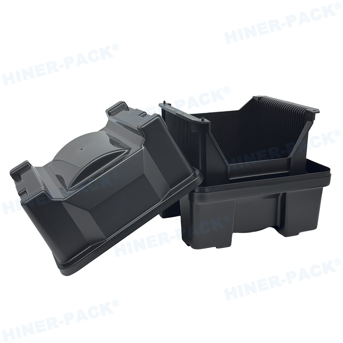
In the domain of advanced semiconductor packaging and wafer-level processing, component handling is no longer a secondary logistical concern—it is a front-line determinant of device reliability, production yield, and long-term field performance. Among the most critical yet often underestimated enablers in this ecosystem is the Conductive chip tray. These specialized carriers serve as the primary interface between delicate silicon dies, automated test equipment (ATE), surface-mount assembly lines, and final shipment. As device geometries shrink and 3D architectures become mainstream, the demand for precision, electrostatic discharge (ESD) safety, and contamination-free environments has elevated the selection of chip trays to a strategic decision. This article provides an authoritative, data-driven examination of conductive chip tray technology, material science fundamentals, industry standards, and best practices—offering actionable insights for engineering, operations, and supply chain leaders.
1. Material Science & ESD Control Mechanisms: Beyond Surface Resistivity
Standard polymer trays, while cost-effective, lack the necessary electrical properties to protect sensitive semiconductor devices from ESD events. The shift toward Conductive chip trays is rooted in the physics of charge dissipation. These trays are typically engineered using carbon-filled polycarbonate, polyetherimide (PEI), or polysulfone blends that achieve surface resistivity values ranging from 10³ to 10⁵ Ω/sq—the sweet spot for static dissipative and conductive behavior. Unlike antistatic materials (10⁹–10¹¹ Ω/sq) which only prevent initial triboelectric charging, conductive trays provide a continuous, low-impedance path to ground, eliminating accumulated charge in milliseconds. This performance is critical for handling devices with gate oxide thicknesses below 20Å, where even 50V of static potential can induce latent damage.
Volume Resistivity vs. Surface Resistivity: Conductive chip trays are engineered to meet both ANSI/ESD S20.20 and IEC 61340-5-1 requirements. A well-designed tray ensures that any static charge dissipates through the tray body to a groundable point, minimizing field-induced damage.
Thermal Stability & Cleanroom Compatibility: Advanced materials maintain dimensional stability across temperatures from -40°C to 150°C, essential for thermal cycling during reliability tests. Additionally, trays are manufactured in Class 10 cleanroom environments to prevent particulate contamination that could lead to wire-bonding defects.
Carbon-Fiber Loading Precision: The dispersion of conductive fillers must be precisely controlled to avoid “hot spots” or non-uniform resistivity, which can create localized electrostatic fields. Premium manufacturers use proprietary compounding techniques to ensure batch-to-batch consistency.
2. JEDEC Standards & Form Factor Compatibility
The semiconductor industry relies on standardized mechanical outlines to enable interoperability across global supply chains. Conductive chip trays are predominantly designed to comply with JEDEC Publication 95 (MO-series) for plastic packages, as well as EIAJ standards for legacy packages. These specifications define critical parameters such as tray matrix size, pocket pitch, cavity geometry, and orientation features for automated pick-and-place equipment. For advanced packages like FCBGA (Flip-Chip Ball Grid Array) and WLCSP (Wafer-Level Chip Scale Package), tray pockets must accommodate solder ball arrays without mechanical stress, while maintaining coplanarity control to prevent ball damage during shipping.
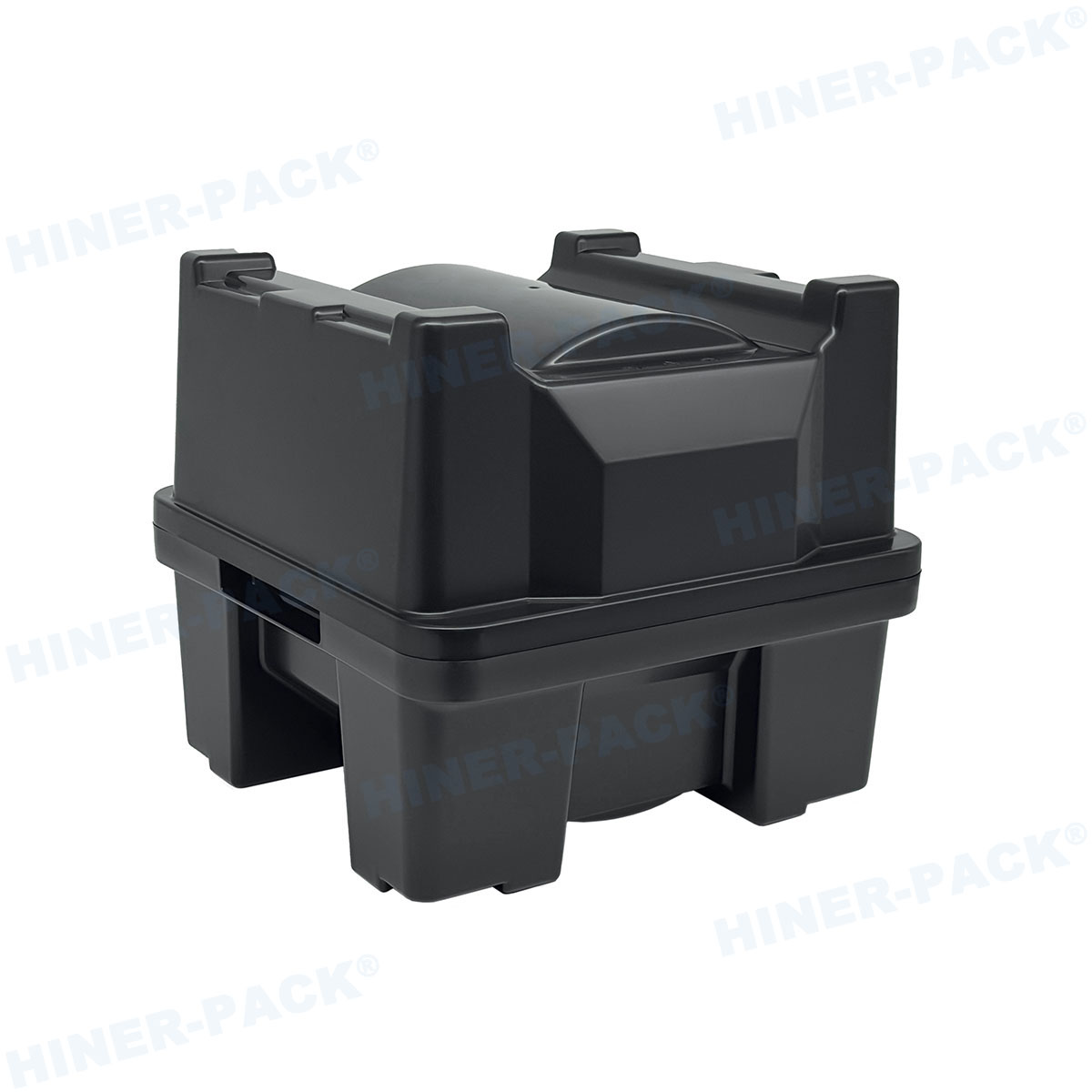
Beyond mechanical fit, modern conductive chip trays integrate features such as anti-rotation ribs, chamfered corners, and stacking ribs that allow secure nesting during automated handling. Compliance with JEDEC Tray Guidelines ensures that trays can be seamlessly integrated into tape-and-reel processes, tube feeders, and magazine loaders without tooling modifications. Hiner-pack offers a comprehensive portfolio of JEDEC-standard and custom-designed Conductive chip trays that undergo rigorous dimensional validation using optical measurement systems—ensuring sub-50µm pocket accuracy.
3. Application Scenarios: From Wafer Probing to Final Assembly
The utility of conductive chip trays spans the entire semiconductor backend process. Each application imposes unique technical demands:
Wafer Sort & Die Preparation: After wafer dicing, individual dies are placed into conductive JEDEC trays for visual inspection, electrical testing, and binning. Trays used in this stage must be fully conductive to prevent static buildup during high-speed die transfer (up to 20,000 units per hour).
Burn-In & Reliability Testing: During high-temperature burn-in (125°C to 150°C), trays must retain ESD properties without outgassing contaminants that could affect test socket contact resistance. Specialized high-temperature conductive chip trays are formulated with glass-reinforced polymers to maintain structural integrity under prolonged thermal stress.
Automated Test Equipment (ATE) Integration: In test floors, trays interface with robotic handlers that index and present devices to test contactors. Tray warpage must be below 0.2mm over the entire matrix to avoid misfeeds. Conductive chip trays with precision-machined alignment features reduce downtime by 18-25% according to field studies from leading OSAT facilities.
Assembly & SMT Lines: For surface-mount technology (SMT) operations, trays are used to present ICs to pick-and-place machines. Conductive materials ensure that moisture-sensitive devices (MSL-rated) are protected from both electrostatic and moisture ingress when stored in dry-pack bags with desiccants.
4. Industry Pain Points & Quantifiable Solutions
Semiconductor fabs and assembly houses routinely encounter yield detractors directly linked to inadequate chip handling. The adoption of high-quality conductive chip trays addresses these pain points with measurable ROI:
ESD-Related Latent Failures: Industry data indicates that up to 30% of field returns in automotive ICs originate from ESD damage during handling that escaped final test. By implementing conductive trays with verified resistivity
<10⁵>Contamination & Particle Generation: Traditional trays fabricated from non-conductive plastics often shed triboelectric particles. Conductive chip trays produced by Hiner-pack undergo ultrasonic cleaning and are certified for particle counts below 1000 particles >0.5µm per tray, meeting Class 100 cleanroom standards. This minimizes visual rejects and wire-bond non-sticks.
Automation Throughput Bottlenecks: Poorly designed trays cause jams in handlers, leading to 1-3% equipment downtime. Advanced conductive chip trays with molded-in fiducials and anti-static coatings ensure smooth operation in leading-edge handlers from Advantest, Teradyne, and ASM. Case studies show a 12% increase in effective uptime after switching to precision trays.
Traceability & Data Integration: Modern smart factories require trays with laser-marked 2D Data Matrix codes to track device genealogy. Conductive chip trays can incorporate high-contrast marking areas without compromising ESD performance, enabling full lot traceability through the supply chain.
5. Why Hiner-pack’s Conductive Chip Trays Set the Benchmark
With over two decades of specialization in semiconductor carriers, Hiner-pack has established itself as a trusted partner for IDMs, OSATs, and EMS providers globally. The company’s engineering approach integrates finite element analysis (FEA) for warpage prediction, mold flow simulation for fill uniformity, and in-line resistivity monitoring for every production batch. Unlike generic suppliers, Hiner-pack offers fully customizable Conductive chip trays tailored to specific package dimensions, handling equipment, and environmental requirements. Their trays are verified to maintain surface resistivity within ±0.5 decades of specification after 500+ cleaning cycles, ensuring long-term performance in high-turnover environments. Furthermore, the company provides comprehensive qualification packages including ESD testing, thermal cycling reports, and outgassing analysis per SEMI standards—delivering the documentation required for automotive (IATF 16949) and aerospace quality systems.
6. Emerging Trends: AI-Driven Handling, Sustainability, and Advanced Materials
The next generation of conductive chip trays is being shaped by three megatrends:
AI-Optimized Tray Logistics: Machine learning algorithms now analyze tray usage patterns to optimize inventory levels and reduce changeover times. Conductive trays with RFID or conductive ink-based identification are enabling real-time tracking within smart factories.
Sustainable Material Formulations: As environmental regulations tighten, the industry is adopting bio-based conductive polymers and recyclable tray systems. New formulations maintain ESD performance while reducing carbon footprint by up to 40% compared to conventional materials.
Heterogeneous Integration Compatibility: With chiplets and multi-die packages, tray pockets must accommodate complex geometries including overmolded components and exposed die backside. Conductive chip trays now incorporate custom elastomeric inserts or multi-level cavities to protect sensitive structures during assembly.
7. Technical Validation: Testing Protocols & Quality Assurance
To ensure reliability, conductive chip trays must undergo stringent validation protocols before deployment. Key tests include:
Surface Resistivity Mapping: Per ANSI/ESD STM11.11, measurements are taken at nine defined points across the tray to confirm uniformity.
Charge Decay Test: Using a charged plate monitor (CPM), trays must dissipate a 1000V charge to below 50V in less than 2 seconds under ambient conditions.
Mechanical Stress Screening: Stacking tests simulate vibration during overland shipping, with acceleration up to 3G, verifying that trays do not crack or deform.
Thermal Cycling: Tray materials are cycled from -40°C to 150°C for 200 cycles while monitoring dimensional stability and electrical properties.
Hiner-pack maintains an in-house NABL-accredited laboratory to perform these validations, providing customers with full traceability and COC (Certificate of Conformance) documentation for each production lot.
Conductive Chip Trays as a Strategic Enabler
In the high-stakes semiconductor industry, yield is measured in basis points, and every handling step carries potential risk. Conductive chip trays have evolved from simple carriers to engineered components that directly impact electrical performance, process efficiency, and supply chain integrity. By leveraging advanced materials, precision manufacturing, and rigorous compliance with JEDEC and ESD standards, manufacturers can eliminate a major source of variability. As a leader in this niche, Hiner-pack continues to drive innovation through custom engineering, cleanroom production, and data-backed quality assurance—enabling customers to achieve best-in-class yields in the most demanding applications.
Frequently Asked Questions (FAQ)
Q1: What is the primary difference between antistatic and conductive chip trays?
Antistatic trays typically have surface resistivity in the range of 10⁹–10¹¹ Ω/sq, which prevents triboelectric charging but does not provide a grounded discharge path. Conductive chip trays, with resistivity below 10⁵ Ω/sq, allow charge to flow rapidly to ground, eliminating electrostatic potential entirely. For sensitive devices such as RF components or advanced CMOS, conductive trays are mandatory to meet ANSI/ESD S20.20 compliance.
Q2: How do conductive chip trays impact overall manufacturing yield?
Yield impact is quantifiable: ESD damage accounts for approximately 20-30% of latent failures in semiconductor devices. By using conductive trays that maintain<10⁵>
Q3: Can conductive chip trays be reused, and what cleaning methods are recommended?
Yes, high-quality conductive chip trays are designed for multiple re-use cycles. Cleaning protocols typically involve deionized water with mild surfactants in ultrasonic baths, followed by Class 10 cleanroom drying. It is critical to verify that cleaning does not alter surface resistivity or introduce ionic contamination. Hiner-pack provides cleaning validation guidelines to ensure trays maintain ESD performance after 200+ cycles.
Q4: What JEDEC standards apply to conductive chip trays, and how do I select the correct tray format?
JEDEC Publication 95 defines the outline dimensions, pocket spacing, and orientation features for trays used with various package families (e.g., MO-019 for TSOP, MO-192 for BGA). Selecting the correct format requires matching the package body size, ball/pad pitch, and handling equipment interface. Hiner-pack offers a cross-reference tool and engineering support to help customers identify the exact JEDEC tray matrix or develop custom solutions for non-standard packages.
Q5: Are conductive chip trays compatible with high-temperature burn-in processes?
Specialized high-temperature conductive chip trays are available, typically manufactured from polyetherimide (PEI) or similar materials with glass transition temperatures above 200°C. These trays maintain dimensional stability and ESD properties during extended burn-in at 150°C. It is essential to select trays explicitly rated for the thermal profile of your burn-in system to avoid warpage or material degradation that could impact device positioning.
Q6: How does Hiner-pack ensure lot-to-lot consistency in conductive chip tray production?
Hiner-pack employs statistical process control (SPC) across injection molding, with real-time monitoring of cavity pressure, material temperature, and resistivity. Every batch is sampled for surface resistivity mapping, dimensional metrology using CMM, and cleanliness verification. Certificates of Analysis (CoA) are provided for each lot, ensuring full traceability and compliance with customer specifications.
For further technical specifications or to request samples of precision-engineered Conductive chip trays, visit the product page or contact the engineering team at Hiner-pack to discuss your application requirements.


