In modern semiconductor manufacturing, the physical carrier that protects
individual die during dicing, sorting, testing, and assembly is often overlooked
— yet it directly impacts yield, reliability, and factory automation uptime.
Semiconductor packaging trays have
evolved from simple plastic moulds into precision-engineered platforms that must
meet stringent requirements for electrostatic discharge (ESD) control, thermal
stability, and dimensional accuracy. As advanced packaging (2.5D/3D, fan‑out,
SiP) pushes the boundaries of miniaturisation, the role of these trays becomes
even more critical.
The Critical Role of Packaging Trays in Semiconductor Manufacturing
Workflow
Semiconductor packaging trays are present at nearly every back-end step:
Wafer dicing: After wafer saw, individual die are picked
and placed into trays (often called “waffle packs” or “gel/elastomer trays”) to
prevent chipping and scattering.
Die sorting and inspection: Trays hold known good dies
(KGD) in precise arrays for automated optical inspection (AOI) and electrical
testing.
Die bonding / placement: Surface-mount technology (SMT)
lines rely on trays that are compatible with pick‑and‑place equipment; pocket
location repeatability is paramount.
Intermediate storage and shipping: Between assembly steps
or during transport to OSATs, trays must protect devices from mechanical shock,
humidity, and electrostatic discharge.
Each step imposes unique demands: high‑temperature resistance during reflow
simulations, ultra‑low outgassing for vacuum environments, and materials that do
not induce ionic contamination. This is where suppliers such as Hiner‑pack differentiate themselves
through rigorous material selection and process control.
Material Science and ESD Compliance: A Delicate Balance
The polymer matrix of a semiconductor packaging tray must satisfy
contradictory requirements: mechanical rigidity, low cost, and permanent ESD
protection without ionic impurities. Common base resins include:
PPS (Polyphenylene Sulfide): High heat deflection
temperature (>260°C), excellent chemical resistance, but needs carbon or fibre
loading for conductivity.
PEI (Polyetherimide): Transparent, inherently
flame‑retardant, often used where visual inspection is needed.
PEEK (Polyether ether ketone): For extreme environments
(continuous use at 240°C) and minimal outgassing; used in aerospace and
high‑reliability automotive dies.
Conductive ABS / PS: Cost‑effective for less demanding
applications, but surface resistivity can drift over time.
To meet ESD standards (ANSI/ESD S20.20, IEC 61340‑5‑1), trays must exhibit
surface resistivity between 105 and 1012 Ω/sq. Below
105 Ω/sq, a tray becomes too conductive and risks shorting live
devices; above 1012 Ω/sq, it behaves as an insulator and allows
tribocharging. Permanent dissipative additives (carbon nanotubes, carbon fibre,
or organic antistats) are preferred over topical coatings, which can flake and
generate particles. Leading manufacturers like Hiner‑pack specify volume‑resistive
compounds to guarantee consistent performance across the tray’s lifetime.
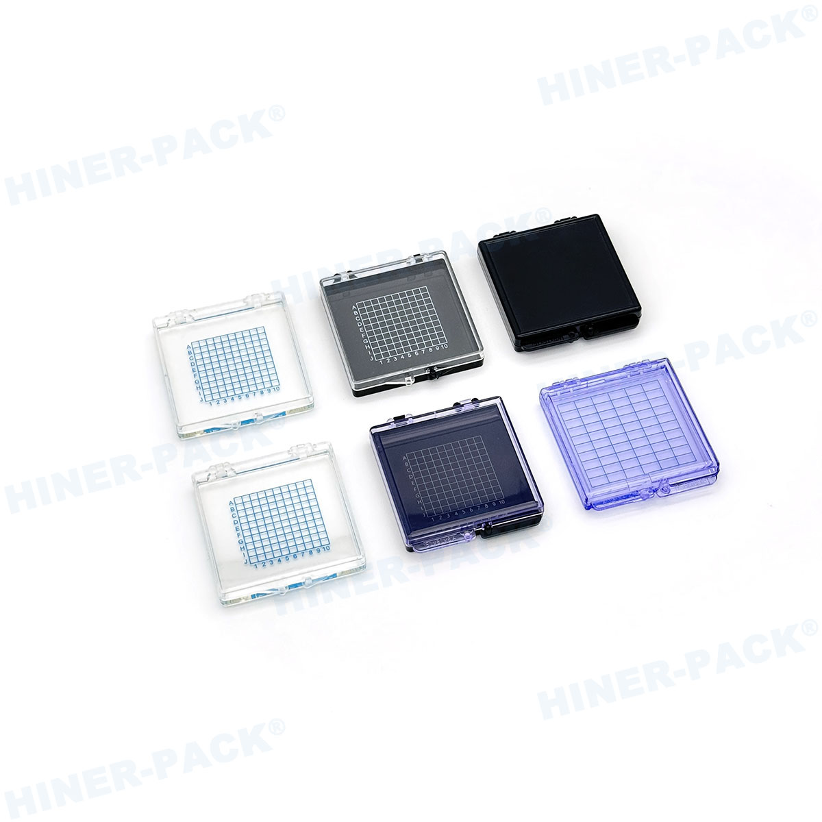
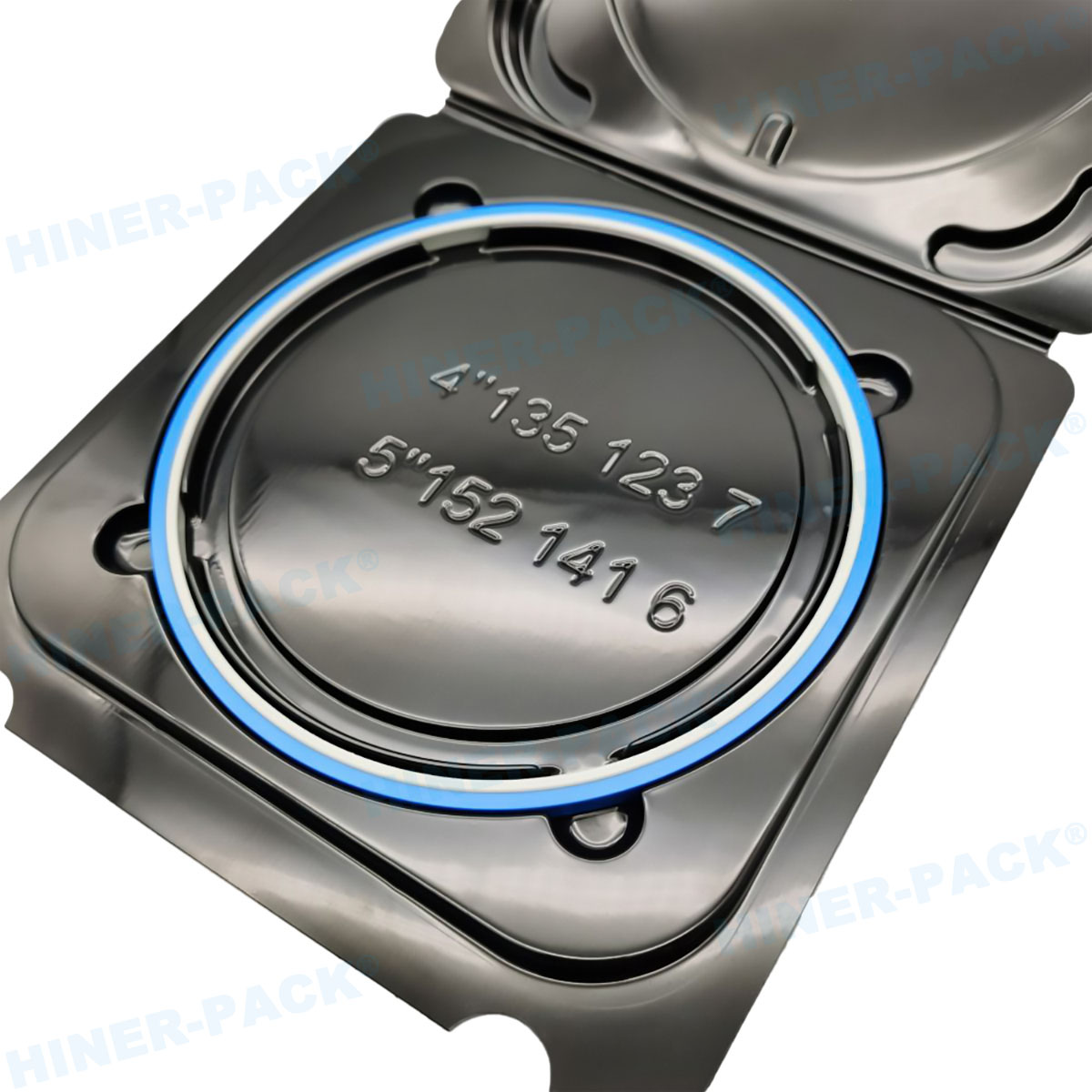
Precision Engineering: Pocket Design, Dimensional Tolerances, and Automation
Compatibility
Pocket Geometry and Chip Protection
Each cavity must secure the die without allowing excessive movement (which
causes chipping) while still enabling vacuum pickup. Modern semiconductor packaging trays employ tapered
sidewalls, rounded corners, and raised “pips” or “bumps” at the pocket bottom to
minimise contact area and prevent stiction. For very thin dies (<50 µm), trays
may incorporate micro‑ribs to distribute stress during thermal cycling.
Alignment Features for Automated Handling
High‑speed pick‑and‑place equipment requires tray registration within ±0.05
mm. Key features include:
Corner cut‑offs / notches: Ensure correct orientation in
stack magazines.
Flatness and coplanarity: Warpage must be less than 0.5% of
diagonal length to avoid misfeeds.
Stackability: Interlocking ribs prevent sliding during
shipping while allowing de‑nesting by robots.
Thermal and Mechanical Stress Considerations
Trays often undergo temperature variations from –40°C (cold storage) to
+150°C (baking). The coefficient of thermal expansion (CTE) should ideally match
silicon (2.6 ppm/K) as closely as possible — a nearly impossible task for
polymers. Instead, designers compensate by leaving clearance around the pocket
and using materials with low moisture absorption (<0.2%) to minimise dimensional
change.
Addressing Industry Pain Points: Contamination, Warpage, and Tray
Reusability
Semiconductor fabs and OSATs face three chronic issues with packaging
trays:
Particle contamination: Friction between trays and handling
equipment can generate particles. Hard coatings or low‑particulate materials
(e.g., PEEK with PTFE fillers) reduce this. Hiner‑pack offers Class‑100
cleanroom compatible trays, verified by laser particle scanning.
Warpage after heat exposure: Moulded‑in stress relief and
proper annealing are essential. Trays should be verified to JEDEC standards
(e.g., JESD22‑B112) for package flatness.
Reusability and cleaning: High‑quality trays can be reused
50–100 times if cleaned correctly. However, aggressive cleaning (ultrasonic,
solvents) may degrade ESD properties. Some suppliers now offer RFID‑tagged trays
to track usage cycles.
Industry Standards and Certification Requirements
Compliance with global standards is mandatory for any semiconductor packaging tray used in tier‑1 fabs. Key
references:
JEDEC Publication 95 (Design Guide 4.14): Dimensional
standards for matrix trays.
EIA‑541: Packaging material standards for ESD sensitive
items.
ANSI/ESD STM11.13: Two‑point resistance measurement of
trays.
RoHS / REACH: Restriction of hazardous substances; many
fabs also require halogen‑free declarations.
Reputable manufacturers like Hiner‑pack provide full
documentation, including ionic cleanliness tests (IPC‑TM‑650) and outgassing
analysis via TD‑GC‑MS, assuring that trays will not contaminate sensitive
devices.
Customization Trends for Advanced Packaging (Fan‑Out, SiP, Heterogeneous
Integration)
As chip designs become more heterogeneous, off‑the‑shelf trays no longer
suffice. Requirements include:
Multi‑pocket depths: For stacked dies or package‑on‑package
(PoP) modules.
Mixed cavity arrays: Different die sizes within one tray to
support high‑mix assembly lines.
Embedded magnets or alignment pins: For automated guided
vehicles (AGVs) in smart factories.
Laser‑marked 2D barcodes: Direct marking on the tray
material (instead of labels) to survive baking and cleaning.
Hiner‑pack leverages CNC machining
and precision injection moulding to deliver custom designs with lead times as
short as two weeks, enabling rapid prototyping for new package outlines.
How Hiner‑pack Delivers High‑Performance Semiconductor Packaging Trays
With decades of experience in the semiconductor supply chain, Hiner‑pack has engineered its
semiconductor packaging trays to meet
the most demanding requirements:
Material portfolio: From PEEK for high‑temperature
processes to carbon‑fibre‑reinforced PPS for cost‑sensitive automotive.
Cleanroom manufacturing: All trays are moulded, handled,
and packaged in ISO Class‑7 (Class 10,000) environments, with optional Class‑5
packaging.
Traceability: Each tray batch is tested for surface
resistivity, flatness, and particle count; certificates are provided.
Global footprint: Distribution centres in Asia, Europe, and
North America ensure just‑in‑time delivery.
Their flagship waffle‑pack chip tray series is widely adopted for MEMS, LEDs,
and logic ICs, offering pocket pitches from 2 mm to 50 mm and depths up to 10
mm.
Future Outlook: Sustainable Materials and Intelligent Trays
The next generation of semiconductor packaging trays will
likely incorporate:
Bio‑based or recycled polymers: PTT (polytrimethylene
terephthalate) and recycled PPS are under evaluation to reduce carbon
footprint.
Smart sensors: Embedding ultra‑thin RFID or even
temperature/humidity loggers to monitor conditions throughout the supply
chain.
Self‑cleaning surfaces: Nanotextures or photocatalytic
coatings that prevent particle adhesion.
As packaging density increases, the tray becomes an integral part of the
factory’s digital twin — its geometry and material properties are simulated to
optimise pick‑and‑place trajectories. Companies like Hiner‑pack are already collaborating
with equipment makers to standardise communication protocols between trays and
robotic handlers.
Frequently Asked Questions (FAQ)
Q1: What is the difference between conductive and dissipative semiconductor
packaging trays?
A1: Conductive trays typically have surface resistivity
below 105 Ω/sq and are used when rapid charge dissipation is needed,
but they risk shorting live circuits. Dissipative trays range from
105 to 1012 Ω/sq, providing controlled drainage of static
charges without arcing. Most JEDEC‑compliant trays are dissipative.
Q2: Can semiconductor packaging trays be cleaned and reused, and if so,
how?
A2: Yes, high‑quality trays from suppliers like
Hiner‑pack are designed for multiple use cycles. Cleaning
methods include deionised water rinsing, isopropyl alcohol (IPA) dips, or
CO2 snow cleaning. However, aggressive ultrasonic cleaning or
abrasive brushes may damage the ESD coating if the tray is only surface‑treated.
Always verify with the manufacturer’s guidelines.
Q3: What material is best for high‑temperature applications (>200°C)?
A3: PEEK (polyether ether ketone) is the industry standard
for continuous use up to 240°C. It exhibits very low outgassing, excellent
chemical resistance, and maintains mechanical integrity during lead‑free reflow
processes. For slightly lower temperatures (<220°C), PPS or PEI are
cost‑effective alternatives.
Q4: How do I ensure my trays are compatible with automated pick‑and‑place
equipment?
A4: Verify that the tray follows JEDEC matrix tray
dimensions (e.g., 2″×2″ to 12″×12″) and that pocket pitch tolerances are within
±0.05 mm. It is also essential to confirm the tray’s flatness (warpage) and the
presence of alignment features like notches or corner radii. Request a
mechanical drawing from your tray supplier and run a first‑article test on your
placement machine.
Q5: What is “outgassing” and why is it critical for semiconductor
trays?
A5: Outgassing refers to the release of volatile compounds
(solvents, plasticisers, moisture) from a polymer when heated. In vacuum
environments or during reflow, these volatiles can condense on bond pads or
optics, causing adhesion failures or corrosion. High‑reliability trays undergo
outgassing tests per ASTM E595, requiring total mass loss (TML) <1% and
collected volatile condensable materials (CVCM) <0.1%.
Q6: Can you provide trays with custom pockets for different die sizes in one
matrix?
A6: Absolutely. Many advanced assembly lines require
multi‑cavity trays to support heterogeneous integration.
Hiner‑pack offers custom‑designed trays with variable pocket
geometries, depths, and even stepped cavities for pre‑stacked modules.
CNC‑machined prototypes can be delivered within days.
For more technical specifications or to request a quote on semiconductor packaging trays tailored to your
devices, visit Hiner‑pack’s official site.


