Within the semiconductor fab, the movement of silicon wafers between process
tools represents a logistical challenge with direct yield implications. The
wafer cassette serves as the foundational carrier, providing secure mechanical support,
standardized automation interfaces, and environmental protection across hundreds
of processing steps. As a B2B content marketing specialist and authority in
international semiconductor wafer processing, I will examine the engineering
rigor, material science, and operational considerations that define modern
wafer cassettes.
This analysis draws from fab-level performance data and addresses how precision
carriers reduce defect densities and enable the transition to advanced
nodes.
1. Material Engineering and Structural Design of Wafer Cassettes
The performance of a wafer cassette is
rooted in its material formulation and mechanical architecture. Modern fabs
demand carriers that withstand thermal cycling, aggressive chemicals, and
continuous automated handling while maintaining sub-micron cleanliness.
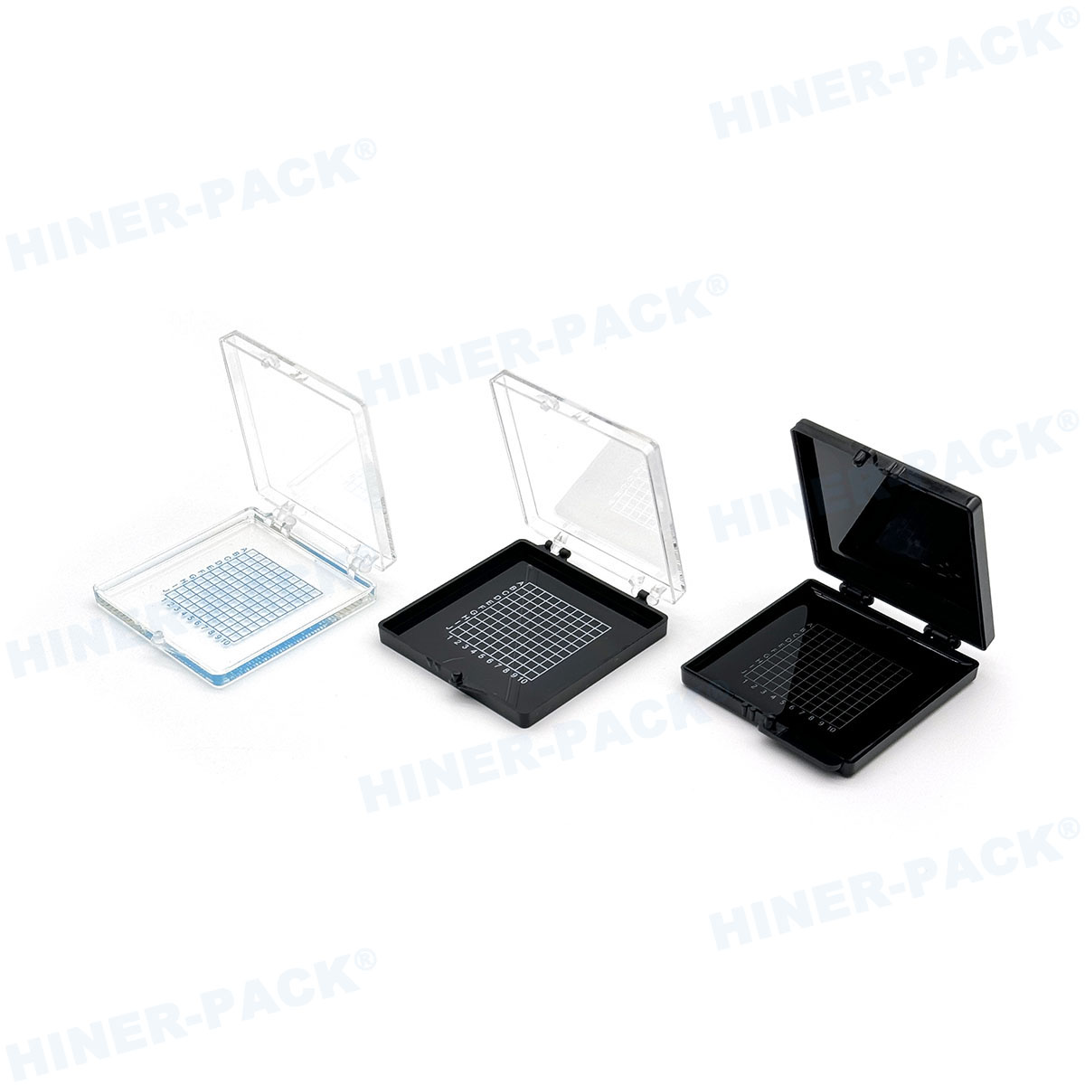
1.1 Polymer Selection for Process Compatibility
Polyetheretherketone (PEEK) remains the benchmark for high-temperature
applications (260°C continuous), particularly in diffusion, CVD, and solder
reflow processes. Its inherent chemical resistance to solvents like NMP and
photoresist strippers prevents degradation and particle shedding. For less
extreme environments, polypropylene (PP) and polycarbonate (PC) offer cost
advantages, but must be compounded with carbon fiber or carbon nanotubes to
achieve the required surface resistivity of 10⁶ to 10⁹ Ω/sq. This
static-dissipative range is specified by SEMI E49 to prevent electrostatic
discharge (ESD) damage without risking charge-induced device failure.
1.2 Dimensional Stability and Automation Interfaces
Automated material handling systems (AMHS) rely on precise mechanical
features. A standard wafer cassette must maintain slot pitch
accuracy within ±0.1 mm after repeated thermal cycles. Finite element analysis
(FEA) is used to optimize rib structures that resist warpage. Key interfaces
include kinematic coupling pockets for load ports, side-rail alignment features,
and bottom notches for conveyor tracking. SEMI E111 and E15.1 define these
mechanical interfaces for 300mm and 200mm carriers, respectively, ensuring
interoperability across equipment from major tool vendors.
2. Critical Applications Across the Semiconductor Workflow
Wafer cassettes are deployed across front-end and back-end processes, each
with distinct technical requirements. Below is a breakdown of application zones
where cassette design directly impacts operational success.
Front-End Processing (Fab): In lithography, etch, and
deposition, cassettes must minimize particle generation during transport.
“Edge-grip” designs that contact only the wafer’s extreme periphery reduce
backside contamination. For ion implantation, cassettes with reduced metal
content and low-outgassing materials prevent dopant contamination.
Wet Process Stations (Cleaning, Etching): Cassettes used in
wet benches require open architectures with drainage channels to prevent
chemical pooling. Materials must withstand pH extremes (from 10% HF to strong
bases) without leaching trace metals. Many fabs now specify cassettes with
smooth, rounded edges to eliminate stress risers that can trap particles.
Thermal Processing (Diffusion, Annealing): High-temperature
cassettes (PEEK or quartz) maintain structural integrity at up to 300°C. Slot
design must accommodate wafer expansion while preventing sticking. Post-process
cooling rates are also influenced by cassette thermal mass—an often-overlooked
factor in cycle time optimization.
Back-End Assembly and Test: For wafer-level packaging (WLP)
and probe testing, cassettes integrate with automatic test equipment (ATE) and
handling systems. Here, ESD protection becomes paramount, as thin-wafer handling
increases sensitivity to electrostatic events. Many advanced cassettes
incorporate embedded conductive pathways to ensure continuous
grounding.
3. Industry Pain Points: Quantifying Risks from Suboptimal Cassette
Performance
Defects originating from wafer carriers account for a measurable portion of
yield loss in advanced nodes. Based on 2024 industry yield reports, below are
the primary technical pain points and their economic implications.
3.1 Particle Contamination and Additive Migration
Friction between the wafer edge and cassette slot can generate submicron
particles. For a 3nm logic process, a single 20nm particle can cause complete
die failure. Each 1% yield loss at a mature 300mm fab translates to
approximately $50M annual revenue impact. High-quality cassettes employ
ultra-smooth slot surfaces (Ra < 0.2 μm) and non-abrasive polymers to
eliminate this. Hiner-pack implements injection
molding processes in ISO Class 4 cleanrooms, with 100% inspection for
particulate contamination using automated optical systems.
3.2 Electrostatic Discharge (ESD) Failures
In dry fab environments (< 40% RH), static charges accumulate on cassettes
and wafers. A discharge below 100V can damage thin gate oxides. Non-homogeneous
static-dissipative materials can create localized charge buildup, leading to
field-induced damage. The solution is cassettes with uniformly dispersed
conductive fillers, ensuring volume resistivity remains stable across
temperature and humidity ranges. Advanced specifications require static decay
times under 2 seconds per MIL-STD-3010.
3.3 Chemical and Thermal Degradation
Repeated exposure to aggressive solvents or high temperatures can degrade
polymer matrices, causing surface roughening and increased particle shedding.
This is particularly problematic in wafer-level packaging where cassettes
undergo multiple reflow cycles. Accelerated life testing (ALT) now simulates 5+
years of fab use to validate material longevity.
3.4 Automation Compatibility and Downtime
Incompatibility between cassette designs and automated load ports leads to
alignment errors, tool alarms, and unscheduled downtime. Each downtime event can
cost over $15,000 per hour in lost throughput. Precision cassettes from
experienced suppliers include first-article inspection reports verifying
conformance to SEMI standards and tool-specific interface requirements.
4. Engineered Solutions: How Advanced Cassette Designs Optimize Fab
Operations
Addressing the aforementioned challenges requires a systems-level engineering
approach. Below are specific technological advancements that define
high-performance wafer cassettes today.
Multi-Material Overmolding: Hybrid cassettes combine a
rigid structural frame (PEEK or PPS) with soft-contact slot inserts made from
thermoplastic elastomers (TPE). This reduces edge contact pressure by up to 60%,
minimizing particle generation while maintaining precise wafer
registration.
Intelligent Traceability: Permanently laser-marked Data
Matrix codes or embedded RFID tags enable full lifecycle tracking. Hiner-pack offers cassettes with
high-contrast barcodes that survive chemical cleaning and thermal exposure,
allowing fabs to correlate defects with specific carrier usage history.
Optimized Fluid Drainage: For wet processing, cassettes are
designed with tapered slots and bottom drainage ports. Computational fluid
dynamics (CFD) modeling confirms these designs reduce drying time by 15–25%,
minimizing watermarks and chemical residue.
Modular Configurations for Thin Wafers: With the
proliferation of thinned wafers (down to 50 μm for 3D-IC), specialized cassettes
feature adjustable slot pitch and gentle retention mechanisms to prevent warpage
or breakage during handling.
Data from a 2024 OSAT (outsourced semiconductor assembly and test) case study
showed that migrating to advanced wafer cassettes with optimized slot geometry and ESD-safe materials reduced assembly-line defect
rates by 18% and increased tool uptime by 9%.
5. Future Trajectories: Smart Carriers, Circular Economy, and
Next-Generation Standards
The evolution of wafer cassettes is being shaped by digital transformation,
sustainability mandates, and tighter SEMI specifications for sub-2nm nodes. As
an industry expert, I foresee the following developments.
5.1 Smart Cassettes with Environmental Sensors
Emerging prototypes integrate thin-film sensors that monitor temperature,
humidity, and shock events throughout the supply chain. Real-time data
transmitted via RFID or Bluetooth allows predictive maintenance and root-cause
analysis for yield excursions, aligning with Industry 5.0 objectives.
5.2 Closed-Loop Recycling Programs
Environmental regulations and corporate net-zero goals are driving demand for
recyclable carriers. Hiner-pack has pioneered a
take-back program where end-of-life PEEK and PP cassettes are reprocessed into
non-critical applications, diverting over 25 tons of engineering plastics from
landfills annually.
5.3 Evolving SEMI Standards for Advanced Nodes
As the industry transitions to 2nm and below, SEMI task forces are revising
standards for airborne molecular contaminants (AMCs) and extractable metals.
Upcoming revisions to SEMI F57 will impose stricter limits on volatile organic
compounds (VOCs) and ionic contaminants, requiring suppliers to adopt advanced
analytical methods (GC-MS, ICP-MS).
Frequently Asked Questions (FAQ)
Q1: What is the difference between a wafer cassette and a FOUP (Front
Opening Unified Pod)?
A1: A wafer
cassette is an open carrier that provides wafer support and
alignment but does not seal the wafers from the fab environment. It is typically
used within process tools or for short-distance manual transport. A FOUP is a
sealed, mini-environment enclosure that protects wafers during automated
transport between tools, incorporating a door, purge ports, and filtration.
FOUPs often contain one or more internal cassettes to organize the wafers.
Q2: How do I select the appropriate material for my wafer cassette
application?
A2: Material selection depends on
three factors: maximum process temperature, chemical exposure, and ESD
requirements. For applications up to 150°C with mild chemicals, anti-static
polypropylene (PP) is cost-effective. For temperatures up to 260°C with
aggressive solvents, PEEK is the industry standard. Always verify outgassing
profiles (via TGA/GC-MS) and surface resistivity to meet your specific cleanroom
class and device sensitivity. Consult with suppliers like Hiner-pack for material data
sheets.
Q3: What are the standard cleaning and requalification protocols for
reusable cassettes?
A3: Reusable cassettes require
cleaning to prevent cross-contamination. Standard protocols involve ultrasonic
cleaning with deionized water and non-ionic surfactants, followed by rinsing and
drying in ISO Class 4 environments. For high-temperature applications, periodic
plasma cleaning may be used to remove organic residues. Requalification includes
particle testing per SEMI E46 and verification of surface resistivity. Many fabs
establish cleaning intervals based on usage cycles (e.g., every 50 process
runs).
Q4: How can I ensure compatibility with my fab’s automated material
handling system (AMHS)?
A4: Verify that the
cassette conforms to SEMI E111 (for 300mm) or SEMI E15.1 (for 200mm)
specifications. Key features include precision kinematic coupling surfaces,
flatness tolerance across the base, and dimensional stability under load.
Request a first-article inspection report and perform a trial run with your
specific load port and overhead transport (OHT) vehicle to confirm smooth
transfer.
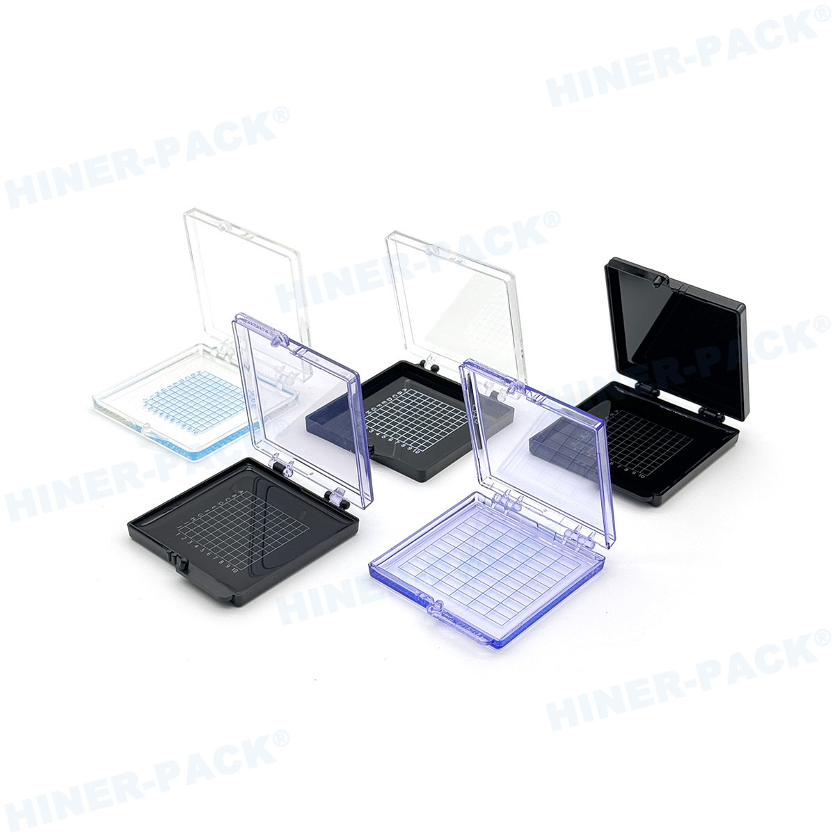
Q5: Can wafer cassettes be customized for non-standard wafer sizes or
specialized process flows?
A5: Yes. For MEMS, power
devices, or R&D applications, custom slot geometries, reduced slot pitches,
and dedicated orientation features are often required. Experienced manufacturers
like Hiner-pack offer
design-for-manufacturing (DFM) support, using 3D CAD models and rapid tooling to
deliver tailored solutions within 4–6 weeks. Customization can also include
specific colors for visual differentiation, RFID integration, and stackability
for high-density storage.
In summary, the wafer cassette is a
precision tool that directly influences semiconductor yield, throughput, and
cost of ownership. From material science to automation compatibility, every
engineering decision carries measurable impact. By adopting advanced materials,
intelligent traceability, and adherence to evolving SEMI standards,
semiconductor manufacturers can mitigate contamination risks, enhance fab
efficiency, and prepare for next-generation nodes. Partnering with established
experts such as Hiner-pack ensures access to
deep domain knowledge and manufacturing excellence required to maintain
competitiveness in this demanding industry.


