In the high-stakes environment of semiconductor fabrication, where feature
sizes shrink below 3nm and defect density requirements approach zero, the humble
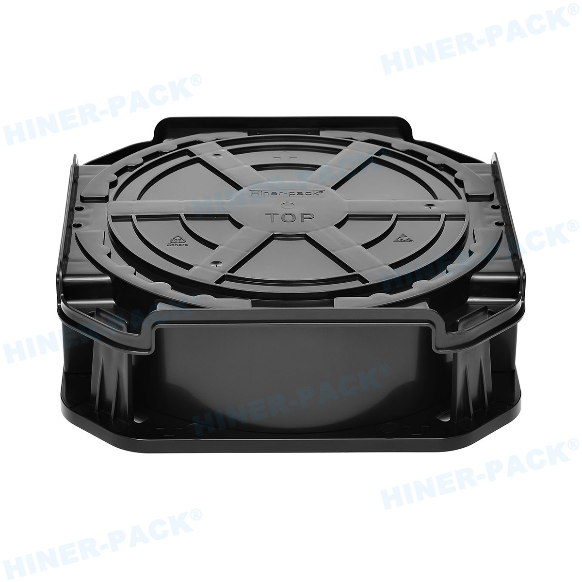
wafer tray transforms into a critical process tool. Far from a simple carrier, modern
wafer trays are
precision-engineered platforms that directly influence yield, throughput, and
device reliability. As a B2B content marketing specialist and authority in
international semiconductor wafer processing, I will dissect the technical
complexities, material science innovations, and application-specific
requirements that define today’s best-in-class wafer handling solutions. This
analysis leverages data from leading fabs and suppliers, emphasizing how
engineered substrate carriers mitigate industry-defining challenges.
1. Material Science & Structural Integrity of Modern Wafer Trays
The selection of materials for a wafer tray dictates
its performance across temperature extremes, chemical exposure, and mechanical
stress. High-volume manufacturing (HVM) demands materials that balance purity,
dimensional stability, and electrostatic discharge (ESD) protection.
1.1 High-Performance Polymers vs. Metal Substrates
While legacy processes sometimes utilize anodized aluminum, the industry has
pivoted toward advanced thermoplastics for 200mm and 300mm wafer trays.
Polyetheretherketone (PEEK) dominates due to its exceptional chemical resistance
to aggressive solvents like NMP (N-Methyl-2-pyrrolidone) and photoresist
strippers, coupled with a continuous use temperature up to 260°C. For less
demanding thermal environments, polypropylene (PP) and polycarbonate (PC) offer
cost-effective solutions with tailored carbon-fiber or carbon-nanotube
formulations to achieve surface resistivity between 10⁶ and 10⁹ Ω/sq—the ideal
range for static dissipation without risking charge-induced device damage.
1.2 Cleanliness and Outgassing Specifications
According to SEMI standards (SEMI F57, SEMI E49), polymeric wafer
trays must exhibit ultra-low levels of extractable metals (e.g., Na, K,
Fe, Cu) and minimal outgassing under vacuum conditions. Advanced injection
molding processes conducted in ISO Class 4 cleanrooms ensure that finished trays
meet or exceed Class 1 particle contamination limits. The industry now demands
laser-marked traceability (Data Matrix codes) directly on the tray body,
enabling full lifecycle tracking—a feature integrated by leading manufacturers
like Hiner-pack to support Industry
4.0 initiatives.
2. Critical Applications Across the Semiconductor Value Chain
A wafer tray is not a
one-size-fits-all component; its design varies dramatically based on process
stage, wafer size (150mm, 200mm, 300mm), and automation interface. Below are key
application zones where tray engineering directly impacts operational
success.
Front-End Processing (Fab): During ion implantation, CVD,
and PVD, wafer trays must withstand high vacuum and thermal cycling. Trays with
reduced contact-area “edge-grip” designs minimize backside contamination and
film deposition on the substrate’s non-active side. Automated guided vehicle
(AGV) compatibility requires precision alignment features with tolerances under
±0.1mm.
Back-End Assembly & Test: In wafer-level packaging
(WLP) and bumping processes, trays are subjected to reflow temperatures up to
260°C and aggressive flux residues. Here, high-temperature PEEK trays with
integrated drainage channels prevent fluid entrapment during spin-rinse-dry
(SRD) cycles.
Wafer Sort and Probe: Electrical testing requires trays
with precise pocket geometries to avoid probe mark damage. Anti-static
properties become paramount to prevent electrostatic discharge (ESD) events that
can destroy sensitive ICs. Many advanced fabs now specify trays with surface
resistivity < 10⁹ Ω/sq and static decay rates < 2 seconds per
MIL-STD-3010.
Inter-fab Logistics and Storage: When wafers are
transported between facilities, trays must be stackable, interlockable, and
compatible with standard FOUP (Front Opening Unified Pod) or FOSB (Front Opening
Shipping Box) interfaces. The trend toward automated material handling systems
(AMHS) demands trays with standardized bottom features for conveyor and stocker
compatibility.
3. Industry Pain Points: Quantifying the Risks of Suboptimal Wafer
Trays
Defects originating from wafer carriers account for a measurable percentage
of yield loss in advanced nodes. Below are the primary technical pain points and
their economic impact, substantiated by industry yield analysis.
3.1 Particle Generation and Additive Contamination
Friction between the wafer and tray surfaces generates submicron particles
that can migrate into active device layers. For a 5nm logic process, a single
30nm particle can render a die non-functional, with each 1% yield loss
translating to millions in annual revenue erosion. High-quality trays employ
non-abrasive, smooth finishes and materials with low coefficient of friction
(COF) to eliminate this. Hiner-pack implements
proprietary molding techniques that produce surfaces with Ra < 0.2 μm,
drastically reducing mechanical abrasion during loading/unloading.
3.2 Electrostatic Discharge (ESD) Failures
In dry cleanroom environments (humidity < 40%), static charges can
accumulate on both the tray and wafer. A discharge event as low as 50V can
damage gate oxides in advanced nodes. Poorly formulated trays lead to
“field-induced” damage or catastrophic ESD. The solution lies in homogenous
static-dissipative materials that maintain consistent resistivity regardless of
humidity. Modern specifications demand volume resistivity below 10⁹ Ω·cm and
static decay times under 0.5 seconds.
3.3 Thermal Dimensional Instability and Warpage
During solder reflow or curing processes (150°C–300°C), differential thermal
expansion between the wafer and tray can induce wafer warpage, leading to
non-contact failures in automated handling. Finite element analysis (FEA) is now
used to design trays with coefficient of thermal expansion (CTE) closely matched
to silicon (2.6 ppm/°C). PEEK compounds filled with carbon fiber achieve CTE
values of 5–8 ppm/°C, minimizing stress.
3.4 Incompatibility with Automation Equipment
With the rise of fully automated fabs, trays lacking standardized alignment
features (e.g., SEMI E111-0712) cause equipment jams and downtime. A single
unscheduled stoppage can cost over $10,000 per hour. Precision-engineered trays
from specialized suppliers ensure 100% compatibility with leading tool vendors
(ASM, K&S, DISCO) and AMHS providers.
4. Engineered Solutions: How Advanced Tray Designs Drive Yield and
Efficiency
Addressing the aforementioned pain points requires a holistic engineering
approach that integrates material formulation, mechanical design, and
data-driven traceability. Below are the specific technological advancements
redefining wafer tray performance.
Multi-Material Co-Molding: Hybrid trays combine rigid
structural frames (PEEK or PPS) with soft-contact “dams” made from thermoplastic
elastomers (TPE). This reduces wafer edge contact stress while maintaining
precise registration, decreasing edge particle counts by up to 70% compared to
single-material designs.
Intelligent Tray Tracking: Embedded RFID tags or permanent
laser-marked 2D barcodes enable real-time inventory management. Hiner-pack offers trays with
high-contrast barcodes readable through chemical exposure and thermal cycles,
ensuring full traceability from incoming wafer inspection to final test.
Optimized Fluid Dynamics: For wet processes (cleaning,
etching), trays are designed with tapered slots and drainage channels that
prevent fluid pooling. Computational fluid dynamics (CFD) simulations validate
that these designs reduce drying time by 15–20%, minimizing watermarks and
chemical residue.
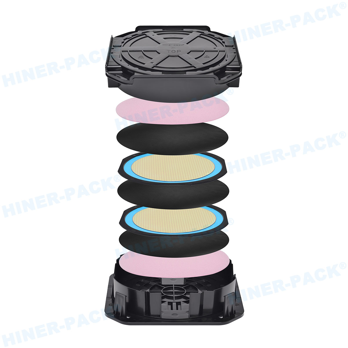
Modular and Scalable Configurations: To accommodate diverse
wafer thicknesses (from 200 μm thinned wafers to 775 μm standard thickness),
adjustable pocket depths and retention features ensure secure transport without
excessive clamping force. This modularity reduces the need for dedicated tray
inventories, lowering tooling costs by up to 30%.
Industry leaders recognize that the cumulative effect of these design
elements yields measurable ROI. A 2023 study by a major OSAT (outsourced
semiconductor assembly and test) provider showed that transitioning to advanced
wafer trays with
integrated ESD control and optimized edge contact reduced their assembly-line
defect rates by 22% and increased tool uptime by 8%.
5. Future Horizons: Smart Trays, Sustainability, and Collaborative
Standards
The next generation of wafer handling solutions will be defined by three
converging trends: digitalization, circular economy, and tighter SEMI
standardization. As an industry expert, I foresee the following developments
reshaping the wafer tray landscape.
5.1 Smart Trays with Embedded Sensors
Prototypes now exist for trays incorporating thin-film sensors that monitor
temperature, humidity, and impact shock throughout the supply chain. Real-time
data transmitted via Bluetooth Low Energy (BLE) or RFID allows predictive
maintenance and root-cause analysis for any yield excursions. This aligns with
the broader smart factory (Industry 5.0) movement.
5.2 Sustainable Material Loops
Environmental regulations and corporate sustainability goals are driving
demand for closed-loop recycling programs. High-performance thermoplastics like
PEEK are increasingly being recycled via certified take-back schemes, reducing
material waste. Hiner-pack has pioneered a
program where end-of-life trays are reground and repurposed into non-critical
applications, diverting over 15 tons of engineering plastic from landfills
annually.
5.3 Evolving SEMI Standards for Advanced Nodes
As the industry moves toward 2nm and beyond, SEMI task forces are updating
standards for wafer carrier cleanliness, outgassing, and ESD. Upcoming revisions
to SEMI F57 will impose stricter limits on volatile organic compounds (VOCs) and
airborne molecular contaminants (AMCs). Suppliers who invest in advanced
analytical testing (GC-MS, ICP-MS) will lead the market.
Frequently Asked Questions (FAQ)
Q1: What is the difference between a wafer tray and a wafer cassette
(FOUP/FOSB)?
A1: A wafer
tray is typically an open, flat carrier designed for single or
multiple wafers during specific process steps (e.g., thermal processing,
plating, test) or for short-distance transport within a tool. In contrast, a
FOUP or FOSB is a sealed, micro-environment enclosure used for automated storage
and inter-equipment transport in the fab. Trays are often placed inside FOUPs or
shipping boxes for added protection, but their primary function is to provide
secure wafer positioning during high-temperature, chemical, or handling
operations.
Q2: How do I choose the right material for my wafer tray
application?
A2: Material selection depends on
three factors: maximum process temperature, chemical exposure, and ESD
requirements. For applications up to 150°C with mild chemicals, anti-static
polypropylene (PP) is cost-effective. For temperatures up to 260°C with
aggressive solvents, PEEK is the industry standard. Always verify the material’s
outgassing profile (via TGA/GC-MS) and surface resistivity to meet your specific
cleanroom class and device sensitivity.
Q3: What are the critical cleaning and maintenance protocols for
wafer trays?
A3: Reusable wafer trays require
regular cleaning to prevent cross-contamination. Standard protocols involve
ultrasonic cleaning with deionized water and non-ionic surfactants, followed by
rinsing and drying in ISO Class 4 environments. For high-temperature
applications, periodic ashing or plasma cleaning may be used to remove organic
residues. It is essential to avoid abrasive brushes that can roughen the surface
and increase particle adhesion. Many suppliers, including Hiner-pack, provide detailed
cleaning validation data.
Q4: How do I ensure compatibility with automated handling systems
(AMHS)?
A4: Verify that the tray conforms to SEMI
E111 (Specification for Mechanical Interface for 300mm FOUP) and relevant 200mm
guidelines. Key features include: precision locating pins or notches, flatness
tolerance across the tray base, and dimensional stability under load. Request a
“first-article” inspection report and perform a trial run with your specific
load port or equipment to confirm smooth transfer.
Q5: Can wafer trays be customized for non-standard wafer sizes or
irregular device shapes?
A5: Yes. For MEMS, power
devices, or R&D applications, custom pocket geometries, cutouts for probe
access, and dedicated orientation features are often necessary. Experienced
manufacturers like Hiner-pack offer
design-for-manufacturing (DFM) support, using 3D CAD models and rapid tooling to
deliver tailored solutions within 4–6 weeks. Customization can also include
specific colors (for visual differentiation), RFID integration, and stackability
for high-density storage.
In conclusion, the wafer tray is a
strategic component that requires the same rigorous engineering as the wafers it
carries. From material selection to smart-tracking capabilities, the choices
made here directly influence yield, cost of ownership, and supply chain
resilience. By leveraging advanced materials, precision design, and adherence to
evolving SEMI standards, semiconductor manufacturers can mitigate contamination
risks, enhance automation compatibility, and prepare for the next wave of
process innovation. Partnering with proven experts such as Hiner-pack ensures access to the
deep domain knowledge and manufacturing excellence required to succeed in this
demanding industry.


