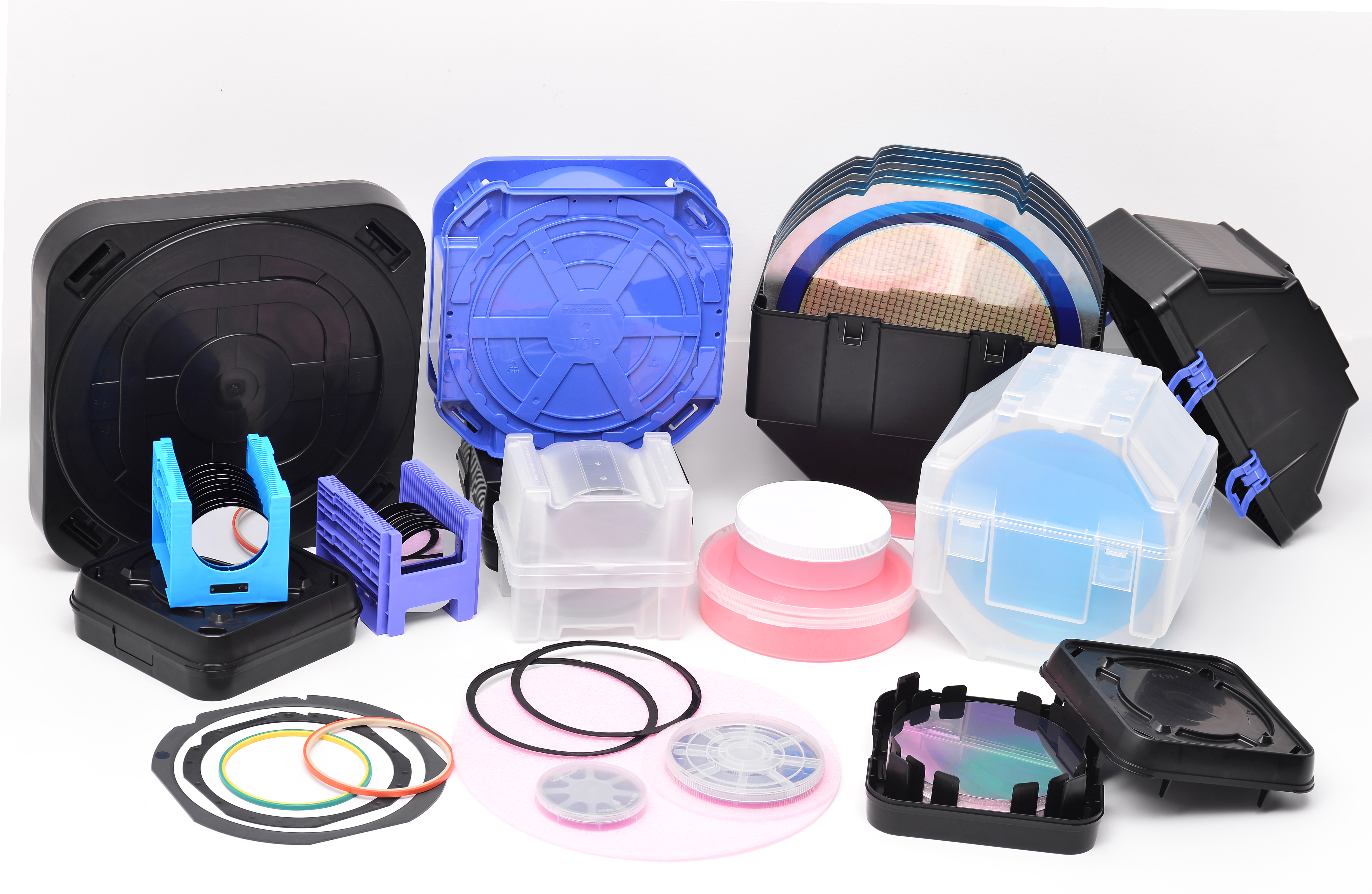
In the intricate landscape of semiconductor fabrication, the wafer
holder represents a nexus of physics, material science, and process
engineering. Often overshadowed by the lithography tools or etch chambers they
inhabit, these components serve as the fundamental interface between the
processing environment and the delicate silicon substrate. For process engineers
and fab managers, the selection of an optimal wafer
holder is not merely a logistical decision; it is a direct lever on
defect density, thermal uniformity, and ultimately, device performance. This
article dissects the technical complexities, material innovations, and strategic
considerations that define modern wafer handling and retention solutions.
The Core Functionality: Beyond Simple Mechanical Retention
At its most fundamental level, a wafer holder must secure a
substrate during processing. However, the demands of sub-5nm node fabrication
have rendered simple mechanical clamping obsolete. Today’s holders must perform
a symphony of functions: providing uniform thermal conduction, minimizing
particle generation, ensuring electrostatic discharge (ESD) safety, and
maintaining absolute planarization under extreme conditions. The shift from
200mm to 300mm and now 450mm wafer diameters has exponentially increased the
challenges of stress management and edge exclusion control, making the holder’s
design a critical factor in intra-wafer uniformity.
Material selection dictates the holder's performance envelope. Traditional
materials like anodized aluminum are giving way to advanced ceramics such as
alumina (Al₂O₃) and yttria-stabilized zirconia (YSZ) due to their superior wear
resistance and chemical inertness. For plasma-rich environments, the holder must
act as a counter-electrode, requiring precise resistivity control to prevent
arcing or micro-contamination. Hiner-pack has observed a
significant industry shift towards monolithic ceramic designs, which reduce
particle traps and offer superior dimensional stability across the 20-300°C
temperature range typical in deposition processes.
Classification by Process Environment
No single wafer holder architecture suits all applications.
The semiconductor manufacturing process flow is segmented into distinct
environmental zones, each demanding a specialized retention strategy.
1. High-Temperature Processing (Diffusion, Annealing, CVD)
In chemical vapor deposition (CVD) and high-temperature annealing steps, the
holder must withstand aggressive chemical species and temperatures exceeding
1000°C. Here, susceptors—a specialized form of wafer holder—are
engineered from silicon carbide (SiC) coated graphite. The SiC coating provides
a chemically inert barrier, preventing metallic contamination while the graphite
core offers lightweight thermal stability. Key technical parameters include:
Thermal Mass Optimization: Balancing heat capacity with
ramp-up rates to maximize throughput without inducing thermal shock
fractures.
Surface Roughness (Ra): Maintaining a Ra below 0.4 µm to
prevent slip dislocations in epitaxial layers.
Pocket Depth Control: Pocket depths are now specified to
tolerances of ±5 microns to minimize wafer backside deposition while ensuring
proper susceptor-to-wafer thermal coupling.
2. Vacuum and Plasma Environments (Etch, PVD, ALD)
In plasma etch and physical vapor deposition (PVD), the wafer
holder transforms into an electrostatic chuck (ESC). ESCs utilize
Johnsen-Rahbek or Coulombic forces to clamp the wafer without mechanical
contact, a necessity for processes requiring strict temperature control under
high vacuum. The engineering challenges here are formidable:
Dielectric Layer Integrity: The dielectric layer must
withstand dielectric breakdown voltages exceeding 2kV while providing consistent
clamping force across the wafer.
Gas Channeling: Helium backside cooling channels are etched
into the surface, requiring labyrinthine seals to prevent process gas incursion.
A 1% variation in helium pressure can translate to a 5°C temperature delta at
the wafer surface, directly impacting etch rate selectivity.
RF Power Delivery: The holder must function as a radio
frequency (RF) electrode, requiring precise impedance matching to maintain
stable plasma density.
Industry Pain Points and The Cost of Failure
The economic impact of a suboptimal wafer holder is severe.
In a 300mm fab, a single wafer lot (25 wafers) can represent $250,000 in value.
Holders that fail to maintain uniformity contribute to three primary categories
of yield loss:
Thermal Runaway: Inconsistent thermal contact leads to hot
spots. For instance, in metal gate deposition, a 3°C variance across the wafer
can shift threshold voltage (Vt) by over 15 mV, causing parametric failure in
high-performance logic devices.
Particle Contamination: Wear particles from the holder,
particularly in moving parts or clamp rings, are a primary source of killer
defects. For a DRAM manufacturer, a single 40nm particle on a critical mask
layer can render an entire die non-functional, with a defect density increase of
just 0.1/cm² costing millions annually in scrap.
Edge Exclusion Inefficiency: As fabs push to utilize more
of the wafer real estate (reducing edge exclusion from 3mm to 1mm), the
mechanical design of the holder’s edge grip becomes critical. Poor edge design
results in non-uniform films, reducing the number of good dies per wafer by up
to 2-3%.
Material Science Innovations: The Shift to Advanced Ceramics and
Coatings
The modern fab requires a wafer holder that is a composite
masterpiece. The trend is moving toward multi-material systems where the core
provides structure, and coatings provide functionality. For example, in atomic
layer deposition (ALD), which operates at lower temperatures but with highly
corrosive precursors, the holder must resist chemical attack from gases like
trimethylaluminum (TMA).
Providers like Hiner-pack have pioneered the
use of yttrium oxide (Y₂O₃) and yttrium fluoride (YF₃) coatings on aluminum and
ceramic holders. These materials offer a plasma etch rate that is an order of
magnitude lower than traditional anodized coatings, drastically reducing
particle contamination in etch chambers. Furthermore, the introduction of
anisotropic surface textures—micro-patterns engineered to reduce contact
area—has enabled holders that actively minimize the Van der Waals forces that
cause stiction, a major issue in vacuum transfer processes.
Engineering for Longevity: Maintenance and Wear Analysis
A strategic approach to wafer holder management involves
predictive maintenance based on cycle counts and electrical signature analysis.
In ESC applications, the DC leakage current is a primary health indicator. A
baseline leakage of < 10 µA at clamping voltage is typical; an increase to
> 50 µA signals impending dielectric breakdown, which can lead to
catastrophic wafer arcing. Fabs now integrate this data into their advanced
process control (APC) systems to schedule consumable replacement without
unscheduled downtime.
Mechanical wafer holders, such as those used in wet processing, face
different degradation vectors. The repeated exposure to acids and solvents leads
to galvanic corrosion at seam lines. Monolithic designs, often sourced from
specialized manufacturers, eliminate these seam lines entirely. The lifecycle
cost (LCC) model is now favored over initial purchase price, with fabs
calculating that a high-quality holder costing 30% more upfront can reduce
consumable-related downtime by 40% over its operational life.
Future Trajectories: Compatibility with Advanced Nodes and New
Materials
As the industry transitions to 3nm and below, and explores substrates like
silicon carbide (SiC) for power electronics and glass core substrates for
advanced packaging, the wafer holder must evolve. The
mechanical properties of glass—specifically its brittleness and transparency to
UV light—render traditional vacuum chucks ineffective. New architectures are
emerging that utilize ultrasonic vibration or porous electrostatic technology to
handle these non-standard substrates without inducing fracture.
Additionally, the rise of high numerical aperture (High-NA) EUV lithography
imposes unprecedented vibration damping requirements. The stage and holder must
now achieve dynamic stability measured in picometers to ensure overlay accuracy.
This demands a fusion of ultra-stiff materials like silicon-infiltrated silicon
carbide (SiSiC) with active damping systems integrated directly into the
holder’s baseplate. The collaboration between equipment manufacturers and
specialist component suppliers is becoming the new paradigm, ensuring that the
wafer holder is not an afterthought, but a co-designed element of the process
architecture.
The wafer holder has
transcended its origins as a simple mechanical component to become a
sophisticated tool for process control. In an industry where margins are
measured in angstroms and defects in parts per billion, the technical
specifications of the interface that secures the wafer are paramount. From the
thermal uniformity requirements of CVD to the electrostatic precision of plasma
etch, the holder is a silent determinant of success. By focusing on material
purity, geometric precision, and process-specific engineering, semiconductor
manufacturers can mitigate yield risks and maximize tool utilization.
Specialized providers like Hiner-pack continue to drive
this evolution, offering engineered solutions that address the most demanding
challenges of next-generation device fabrication.
Frequently Asked Questions (FAQ)
Q1: How does the choice of wafer holder material
affect defectivity in a plasma etch process? A1: The material directly influences particle generation and
metallic contamination. For plasma processes, using a holder with a yttria-based
coating (Y₂O₃) rather than anodized aluminum reduces particle adders by up to
60%, as yttria exhibits significantly lower sputter yield under ion bombardment.
Additionally, it prevents the release of aluminum fluoride (AlF₃) residues,
which are common contaminants that cause via chain failures in backend-of-line
(BEOL) interconnect layers.
Q2: What is the difference between a mechanical
clamp ring and an electrostatic chuck (ESC) for wafer holding? A2: A mechanical clamp ring physically contacts the wafer
edge to hold it in place, which is effective for some processes but introduces
edge exclusion area and potential particle sources from friction. An ESC uses an
electrostatic force to clamp the wafer without edge contact, providing superior
wafer area utilization and temperature control via helium backside cooling. ESCs
are mandatory for processes requiring tight thermal uniformity (< ±1°C) under
high vacuum, such as in advanced etching and deposition.
Q3: How frequently should a wafer holder be replaced
in a high-volume manufacturing fab? A3: Replacement intervals are process-specific and driven by
RF hours or total wafer starts. In a high-density plasma etch chamber, a silicon
carbide or alumina holder might last 20,000-30,000 RF hours, while an ESC’s
dielectric layer typically requires refurbishment after 50,000-100,000 clamping
cycles. Predictive maintenance using in-situ monitoring of leakage current (for
ESCs) or particle counts is the standard to prevent unscheduled
downtime.
Q4: Can a standard wafer holder be used for both
200mm and 300mm wafer processing? A4: No. Holders are designed with specific diameter pockets
and edge grip mechanisms that are not interchangeable between 200mm and 300mm
platforms. However, some advanced process tools allow for "step-down" adapter
kits, but these are specialized and require recalibration of the tool's robot
transfer mechanisms and thermal models to ensure process uniformity. Using the
incorrect holder risks wafer breakage or severe misprocessing.
Q5: What role does the wafer holder play in
preventing wafer breakage during rapid thermal processing (RTP)? A5: In RTP, the holder (often a quartz or SiC edge ring)
acts as a thermal buffer and mechanical support. It is critical in managing the
temperature gradient between the wafer center and edge during temperature ramp
rates exceeding 200°C per second. A holder with optimized edge contact prevents
slip dislocations and warpage by ensuring the wafer expands and contracts
uniformly, distributing thermal stress evenly rather than concentrating it at
the contact points.


