In the race toward sub-2nm nodes and heterogeneous integration, the
carrier
wafer has transitioned from a simple handling substrate to a
sophisticated enabler of high-density interconnect architectures. For
engineering teams and procurement specialists in the semiconductor ecosystem,
understanding the interplay between carrier
wafer material properties, temporary bonding adhesive systems, and
thermal budget management is no longer optional—it is the defining factor
between first-pass yield success and catastrophic delamination in fan-out
wafer-level packaging (FOWLP) and 3D IC stacks. This analysis dissects the
physics, metrology challenges, and supply chain nuances that dictate
carrier wafer selection for high-volume manufacturing
(HVM).

1. The Structural Imperative: Why Carrier Wafers Define Modern Packaging
Roadmaps
The fundamental challenge in advanced packaging is mechanical fragility.
Thinned device wafers—often ground to thicknesses below 50 µm—lack the rigidity
required for photolithography, dielectric deposition, and solder reflow
processes. A carrier wafer serves as a temporary or permanent
foundation that absorbs thermo-mechanical stress during processing. However, the
industry is bifurcating: while traditional fan-out processes rely on temporary
carrier wafers (de-bonded after back-end processing), emerging
applications in chiplet integration and silicon photonics demand permanent
carrier substrates with matched coefficients of thermal expansion (CTE).
Data from leading OSATs indicate that improper carrier wafer selection accounts for up to 18% of yield loss in advanced packaging lines,
primarily due to wafer bow, edge chipping, and adhesive residue contamination.
This statistical reality underscores why process engineers must evaluate carrier
solutions not merely as consumables, but as critical path components.
2. Material Science Deep Dive: Silicon, Glass, and Engineered CTE
Substrates
2.1 Silicon Carrier Wafers: The Baseline Benchmark
Silicon remains the dominant material for carrier wafers due
to its CTE compatibility with device wafers (2.6 ppm/K), availability in 300 mm
diameters, and seamless integration with existing fab tooling. However,
silicon’s opacity poses challenges for laser de-bonding systems requiring
optical transparency. Furthermore, the high dielectric constant (εr ≈ 11.9) of
silicon carriers introduces parasitic capacitance in high-frequency RF
applications, forcing design teams to consider alternative substrates for 5G
mmWave modules.
2.2 Glass Carriers: The Shift Toward Optical Transparency and Electrical
Neutrality
Glass carrier wafers have gained significant traction in
panel-level packaging (PLP) and FOWLP due to their inherent flatness (<0.5 µm
total thickness variation) and tunable CTE (3–8 ppm/K). For processes requiring
laser-assisted de-bonding, glass carriers offer >90% transmittance at 355 nm
wavelength, enabling high-throughput lift-off. The primary trade-off lies in
fracture toughness: glass carriers are more susceptible to edge impact during
automated handling, necessitating specialized edge-grip end effectors and
enhanced cleanroom protocols.
2.3 Advanced Composite Carriers
For extreme temperature excursions—such as those encountered in copper hybrid
bonding (400°C+)—engineered composite carrier wafers combining
silicon cores with dielectric coatings are emerging. These hybrid solutions
mitigate wafer bow by balancing compressive and tensile stress layers, a
critical requirement for 3D stacking where cumulative stress from multiple
thin-film layers can exceed 1 GPa.
3. Temporary Bonding and De-Bonding Technologies: The Interface That
Determines Success
The carrier wafer is only as effective as the adhesive
system that bonds it to the device wafer. Three primary methodologies dominate
HVM environments:
Thermoplastic Adhesives: Offer high thermal stability (up
to 350°C) but require precise temperature-controlled slide de-bonding, which
introduces shear stress risks for ultra-thin wafers.
Laser-Releasable Adhesives: Enabled by glass carriers, this
approach uses a sacrificial layer that decomposes upon UV laser exposure. The
primary advantage is room-temperature de-bonding, eliminating thermal shock.
However, capital expenditure for laser de-bonding tools exceeds $1.2M per 300 mm
line.
ZoneBOND™ and Edge-Trim Methods: A hybrid approach where
only the wafer perimeter is bonded, reducing adhesive material costs by 40% and
simplifying de-bonding, albeit with limitations in edge bead removal
uniformity.
In a 2024 industry survey of 12 major semiconductor fabs, 67% of respondents
cited adhesive residue control as the top technical challenge when implementing
new carrier wafer processes. Residue particles as small as 3 µm
can cause non-wet defects in subsequent copper pillar plating, necessitating
advanced plasma cleaning steps that add 8–12 seconds of cycle time per
wafer.
4. Industry Pain Points: Warpage, Edge Defects, and Metrology Gaps
4.1 Warpage Propagation in Multi-Die Systems
As package architectures move toward 4x and 6x reticle sizes (over 2,500
mm²), cumulative warpage from multiple carrier wafers and
interposers exceeds 3 mm at room temperature, causing focus errors in stepper
scanners. Mitigation requires dynamic wafer chucking systems with adaptive
vacuum zoning, combined with finite element analysis (FEA) simulations that
model warpage through each thermal cycle. Simulation data reveals that
optimizing the carrier wafer thickness from 775 µm to 925 µm
can reduce bow by 34% in multi-wafer stacks.
4.2 Edge Chipping and Defectivity
The interface between the carrier wafer and device wafer is
most vulnerable at the bevel edge. Mechanical de-bonding forces often propagate
cracks from edge defects. Leading-edge fabs now employ bevel-trimming modules
that remove 2–3 mm of the adhesive ring and carrier edge prior to de-bonding,
reducing edge particle adders by a factor of 10x.
4.3 Metrology Challenges for Opaque Carriers
Traditional optical overlay metrology fails when using silicon
carrier wafers due to substrate opacity. This has driven
adoption of infrared (IR) transmission metrology and through-silicon via (TSV)
alignment targets that can be read from the backside. The capital cost for IR
overlay systems is 30% higher than conventional tools, creating a cost barrier
for smaller packaging houses.
5. Cost Modeling: Total Cost of Ownership (TCO) for Carrier Wafer
Programs
While the unit price of a carrier wafer ranges from $40
(reclaimed silicon) to $180 (precision-ground glass), TCO analysis must account
for reusability. Silicon carriers can be chemically stripped and reused 5–8
times in volume production, reducing effective cost per wafer to $6–$10. Glass
carriers, due to surface wear from laser de-bonding, typically achieve only 3–4
reuse cycles. However, the elimination of adhesive clean steps in glass-based
processes can reduce chemical consumption by up to 50%, offsetting higher
carrier costs.
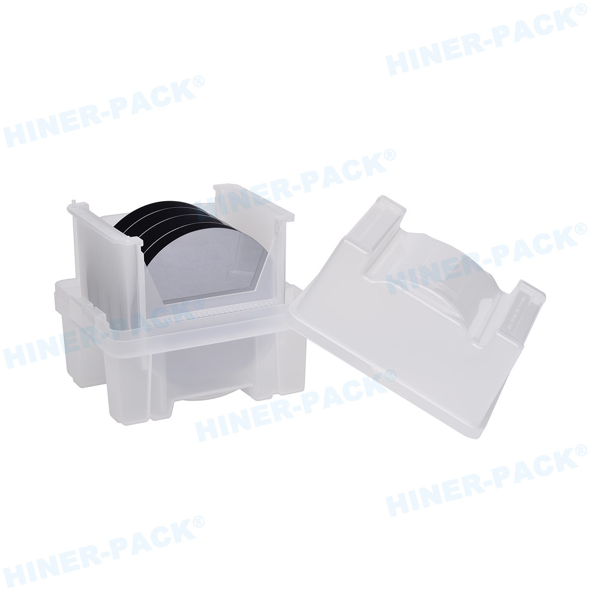
For companies like Hiner-pack, which
specializes in precision wafer handling and packaging logistics, the shift
toward reusable carrier wafers has necessitated the development
of certified cleaning protocols that meet ISO Class 4 cleanliness standards.
Their infrastructure ensures that carriers returned from assembly lines maintain
particle counts below 0.03 particles/cm² for >0.2 µm residues, a critical
factor for yield-sensitive customers.
6. Application-Specific Carrier Strategies
6.1 Fan-Out Wafer-Level Packaging (FOWLP)
In FOWLP, the carrier wafer serves as the temporary
substrate for molding compound formation. The industry is transitioning from 300
mm round carriers to 510 mm x 515 mm rectangular panels to improve die
utilization. However, rectangular carriers introduce new challenges in edge
uniformity and require retrofitting of deposition tools.
6.2 3D IC with Through-Silicon Vias (TSVs)
TSV reveal processes involve thinning the device wafer to expose copper vias
while it is mounted on a carrier wafer. The carrier must
provide sufficient rigidity to withstand chemical mechanical polishing (CMP)
pressures exceeding 5 psi. Silicon carriers with high Young’s modulus (130 GPa)
remain preferred here, as glass carriers risk breakage under the non-uniform
pressure of CMP platens.
6.3 Advanced Heterogeneous Integration (Chiplets)
For multi-chiplet assemblies, carriers are increasingly being designed as
permanent interposers with integrated passive devices (IPDs). This blurs the
line between a carrier wafer and a functional substrate,
requiring embedded thin-film resistors and high-density routing (line/space <
2 µm).
7. Supply Chain and Quality Assurance Considerations
The post-COVID semiconductor supply chain has highlighted vulnerabilities in
carrier wafer availability. Silicon carrier production competes
for capacity with prime device wafers, leading to lead times exceeding 26 weeks
for virgin silicon carriers. To mitigate this, advanced packaging fabs are
adopting carrier reclamation programs where used carriers are stripped,
polished, and requalified. These programs require rigorous metrology checks for
thickness variation (TTV < 2 µm) and nanotopography to prevent pattern
transfer issues.
Hiner-pack has addressed these supply chain
constraints by implementing a closed-loop logistics system that tracks each
carrier wafer’s lifecycle—from initial quality inspection to
reclamation cycles—using RFID-enabled wafer boxes. This system provides
customers with real-time visibility into carrier inventory health and historical
defect data, aligning with the industry’s push toward digital twin integration
in manufacturing operations.
8. Future Outlook: Permanent Carriers and 3D System-on-Wafer
Looking toward the 2030 roadmap, the distinction between carrier and device
is dissolving. Intel’s “System-on-Wafer” and TSMC’s “Integrated Chiplet Stack”
(ICS) technologies propose using silicon carrier wafers as the
foundational substrate for multiple active dies, incorporating power delivery
networks and thermal dissipation structures directly into the carrier. This
paradigm demands carriers with embedded deep trench capacitors (DTC) and
microfluidic cooling channels—features that are currently prototyped using 300
mm wafer-level processes.
Simultaneously, the industry is standardizing carrier interface protocols
under the JEDEC JC-70 committee. Emerging standards will define mechanical
specifications for carrier-to-equipment docking, aiming to reduce tooling
changeover time from 45 minutes to under 10 minutes, enabling more flexible
mixed-production lines.
Carrier Wafers as Strategic Differentiators
For semiconductor professionals, the carrier wafer is no
longer a passive support structure but a strategic lever for yield improvement,
cost reduction, and advanced node enablement. The confluence of material science
innovations, metrology advancements, and supply chain optimization dictates that
organizations must treat carrier selection with the same rigor applied to
lithography and etch processes. As the industry pushes the boundaries of
die-to-die interconnect density, those who master the physics of the carrier
interface will secure a decisive competitive advantage in the heterogeneous
integration era.
---
Frequently Asked Questions (FAQs)
Q1: What is the primary difference between a temporary carrier wafer
and a permanent carrier wafer in semiconductor packaging?
A1: A
temporary carrier wafer is used to support a thinned device
wafer during back-end processing (e.g., dielectric deposition, solder bumping)
and is removed via thermal slide or laser de-bonding before final singulation. A
permanent carrier remains as part of the final package, often serving as an
interposer or mechanical reinforcement in 3D stacks. Permanent carriers require
CTE matching with silicon devices to avoid stress-induced reliability failures
over the product lifetime.
Q2: How does carrier wafer flatness impact overlay accuracy in
fan-out wafer-level packaging?
A2: Carrier wafer total thickness
variation (TTV) directly affects the global planarity of the reconstituted
wafer. For FOWLP, TTV must be maintained below 2 µm across the 300 mm diameter
to ensure that lithography steppers can achieve <1 µm overlay accuracy.
Exceeding this tolerance results in defocus errors, leading to open circuits in
redistribution layers (RDL) and a 5–12% yield drop in high-density fan-out
lines.
Q3: Can silicon carrier wafers be reused, and what cleaning processes
are required?
A3: Yes, silicon carrier wafers can
typically be reused 5–8 times in HVM. After de-bonding, the carrier undergoes
chemical stripping to remove residual adhesives (often using NMP or proprietary
solvent blends), followed by double-side polishing to restore surface roughness
to <0.5 nm Ra. Strict particle control is critical; reclaimed carriers must
pass an optical inspection for scratches and residual metal contamination (e.g.,
Cu < 1e10 atoms/cm²) before re-entry to the fab.
Q4: What are the main causes of adhesive residue contamination from
carrier wafers, and how can they be mitigated?
A4: Residue primarily
originates from adhesive migration at the wafer edge during high-temperature
curing cycles (typically 250°C–350°C). Mitigation strategies include
implementing edge bead removal (EBR) processes that strip adhesive 2–3 mm from
the bevel, optimizing plasma cleaning parameters (e.g., O2/CF4 mixtures) to
achieve complete residue removal, and using UV-curable adhesives with lower
outgassing profiles. Regular SEM inspection of the device wafer edge after
de-bonding is recommended for process control.
Q5: How do glass carriers compare to silicon carriers in terms of
cost per wafer processed?
A5: While the initial purchase price of a
glass carrier wafer is 30–50% higher than a reclaimed silicon
carrier, glass enables laser de-bonding which reduces adhesive chemical costs
and eliminates thermal stress on ultra-thin wafers. A TCO analysis for a
high-volume 300 mm line shows that glass carriers achieve break-even at 2,500
wafer starts per week due to improved yield (+2.3%) and 15% faster cycle times.
However, silicon remains more cost-effective for lower volumes or where IR
alignment is required.
Q6: What role does Hiner-pack play in carrier wafer logistics and
quality management?
A6: Hiner-pack provides
specialized wafer shipping and storage solutions that incorporate ESD-safe
materials and real-time contamination monitoring for carrier
wafers. Their closed-loop tracking system ensures that carriers are
traceable through reclamation cycles, with automated inspection data integrated
into customer MES platforms, reducing the risk of using degraded carriers in
critical process steps.


