The semiconductor supply chain is a global network where time and integrity
are measured in nanometers and parts per billion. While the industry rightly
obsesses over cleanroom purity and process tool precision, the journey between
fabrication facilities remains a zone of extreme risk. The wafer
shipping box, often perceived as a mere commodity, is in fact the
last line of defense against yield loss. For fabless semiconductor companies,
OSATs (Outsourced Semiconductor Assembly and Test), and foundries, the design,
material, and cleanliness of this carrier dictate whether wafers arrive intact
and uncontaminated. This analysis explores the rigorous engineering, material
science, and industry standards governing the containers that protect the
industry’s most valuable substrates during transit.
From Simple Tray to Engineered Environment
The evolution of the wafer shipping box mirrors the
increasing fragility and value of its cargo. In the era of 150mm and 200mm
wafers, simple injection-molded trays with foam inserts were common. Today, with
300mm and 450mm wafers supporting nodes below 5nm, the container has transformed
into a precision-engineered microenvironment. The modern shipping solution must
manage three primary threats: mechanical shock, electrostatic discharge (ESD),
and particulate contamination.
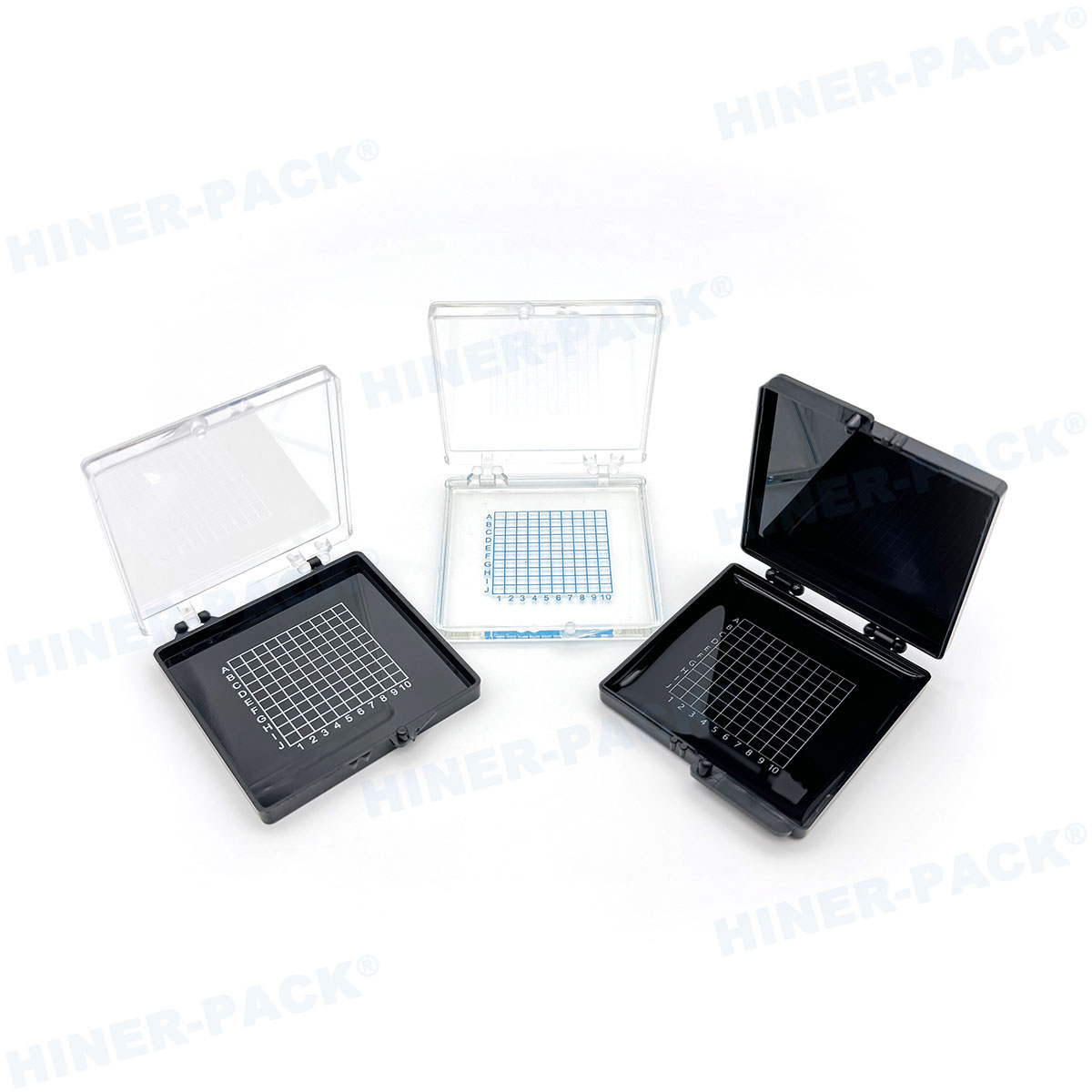
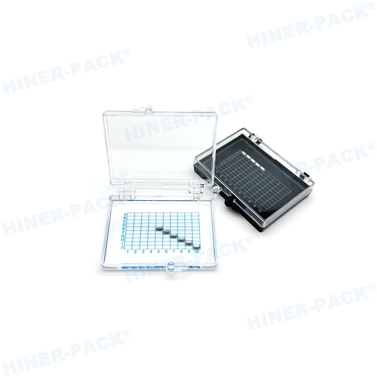
Advanced shipping boxes now incorporate multi-layer structures. The outer
shell, typically constructed from polycarbonate or static-dissipative ABS,
provides structural rigidity against crushing forces defined by ASTM D4169
(Standard Practice for Performance Testing of Shipping Containers). The inner
insert, often a custom-molded wafer cassette or “boat,” is designed to cradle
the wafer stack. The interface between the wafer edge and the retention features
is a focal point of engineering, with contact geometry optimized to prevent
chipping—a critical concern as wafer thickness is reduced to 775 µm for 300mm
substrates and even thinner for stacked memory applications.
Classification by Environment: Standard, Nitrogen-Purged, and Vacuum-Sealed
Solutions
The selection of a wafer shipping box is dictated by the
wafer’s process stage and sensitivity to environmental factors. The industry
categorizes these solutions into three primary tiers, each with distinct
technical specifications.
1. Standard Static-Dissipative Carriers (Front Opening Shipping Box –
FOSB)
The FOSB has become the industry standard for 300mm wafer logistics. Designed
to interface directly with automated material handling systems (AMHS) and
standard mechanical interface (SMIF) pods, the FOSB is more than a shipping
container; it is a standardized transport interface. Key attributes include:
Material Resistivity: Surface resistivity is precisely
controlled within the range of 10⁶ to 10⁹ ohms/sq to prevent static charge
accumulation that could damage gate oxide layers.
Cleanroom Compatibility: The materials are formulated to
minimize outgassing of volatile organic compounds (VOCs) like siloxanes, which
can condense on wafer surfaces and cause haze or adhesion failures in subsequent
lithography steps.
Mechanical Interchangeability: Dimensional tolerances
conform to SEMI E111 (Specification for 300mm FOUP and FOSB) to ensure
compatibility with load ports and robotic systems globally.
2. Nitrogen-Purged and Controlled Atmosphere Boxes
For wafers requiring protection from oxidation, moisture, or airborne
molecular contaminants (AMCs), the wafer shipping box must
maintain a controlled inert atmosphere. These are often referred to as “purge
boxes.” The engineering challenges here are substantial:
Gas Flow Dynamics: The box incorporates
precision-engineered ports that allow for nitrogen or clean dry air (CDA)
purging, displacing ambient air. The internal geometry is designed to prevent
dead zones where moisture or contaminants could reside.
Moisture and Oxygen Barriers: Advanced seals, often
dual-lip silicone gaskets, maintain internal relative humidity below 1% and
oxygen levels below 50 ppm for extended periods. A failure in the seal integrity
of 0.1mm can allow enough moisture ingress to cause native oxide growth on
copper or cobalt interconnects, leading to bond pad corrosion.
Chemical Filtration: Some high-specification boxes
incorporate internal chemical filters (such as activated carbon or ion exchange
media) to adsorb AMCs like sulfuric oxides (SOx) or ammonia, which are known to
cause pattern collapse in immersion lithography.
Material Science and Contamination Control
The materials used in a wafer shipping box must be chosen
with the same rigor as process chamber components. Polyetheretherketone (PEEK),
polypropylene (PP), and polycarbonate (PC) are common base resins, but the
critical factor lies in the additive package used to achieve static dissipation.
Traditional carbon-black fillers, while conductive, can shed particles. The
industry is shifting toward inherently dissipative polymers (IDPs) that provide
consistent ESD protection without the risk of carbon particulate shedding.
For advanced nodes, the specification goes beyond particle shedding to
include ionic cleanliness. Post-molding cleaning processes must achieve
extractable ion levels (chloride, fluoride, sodium) measured in parts per
trillion (ppt). A high-performance wafer shipping box from a
specialist manufacturer like Hiner-pack will often come with
a certificate of analysis verifying that outgassing and ionic contamination are
below the thresholds established by SEMI E150 (Standard for the Measurement of
Airborne Molecular Contamination).
Industry Pain Points: Handling, Shock, and Vibration
Physical damage during logistics remains a primary cost driver. Wafers are
susceptible to two distinct physical phenomena during transport: macro-shock
(from drops or impacts) and micro-vibration (from road or air freight).
Macro-Shock Protection: A drop from just 30 cm can generate
g-forces exceeding 1,000 Gs on the wafer edge if the wafer shipping
box lacks adequate cushioning. Modern designs utilize “floating”
cassette suspension systems, where the inner wafer boat is decoupled from the
outer shell via elastomeric dampers or spring mechanisms that absorb impact
energy before it reaches the wafer.
Micro-Vibration and Fretting: Sustained vibration during
air freight (which operates in the 5-500 Hz range) can cause fretting between
wafers. Even with separation, microscopic movement can generate silicon or
coating dust. The solution involves precision-machined wafer slots with
controlled slot pitch and surface texturing to minimize lateral movement while
maintaining a safe separation gap—typically 6.35 mm for 300mm wafers, as defined
by SEMI standards.
Thermal Cycling: Wafers may transit from a 22°C fab to a
-40°C cargo hold at altitude. The box must manage differential thermal expansion
between the plastic container and the silicon wafers to prevent warp or
cracking. This requires the use of materials with coefficients of thermal
expansion (CTE) closely matched to silicon, or designs that allow for compliant
movement.
The Economics of Failure: Yield Loss in Transit
The true cost of an inadequate wafer shipping box is not the
price of replacement packaging; it is the value of the wafers damaged or
contaminated. A single 300mm wafer can hold over 700 high-performance computing
(HPC) dies, with a value exceeding $15,000. In a high-volume scenario, a failure
rate of 0.1% due to shipping damage translates to millions in annual loss. This
economic reality drives the adoption of rigorous testing protocols,
including:
ISTA 3A or 3E Testing: These International Safe Transit
Association protocols simulate actual distribution hazards, including
compression, vibration, and drop sequences. A certified wafer shipping
box must demonstrate that the wafers remain undamaged and particle-free
after these tests.
Barcode and RFID Integration: Modern logistics require
traceability. High-end carriers incorporate RFID tags that record shock events
(via embedded accelerometers) and temperature breaches. This data allows for
forensic analysis if a wafer lot is flagged for yield issues
post-receipt.
Future Trends: Sustainability and Intelligent Containers
The next generation of wafer shipping solutions is being shaped by
sustainability mandates and the demands of Industry 4.0. Single-use packaging is
increasingly viewed as unsustainable; therefore, there is a strong trend toward
closed-loop, returnable systems managed by logistics specialists. These systems
require boxes designed for high-cycle durability (up to 50 or more trips) with
replaceable components like seals and filters.
Furthermore, the integration of Internet of Things (IoT) sensors is becoming
standard. A “smart” wafer shipping box now can provide
real-time location tracking, humidity logging, and shock detection directly to a
cloud-based platform. For manufacturers shipping sensitive devices like
Micro-Electro-Mechanical Systems (MEMS) or image sensors, this real-time
visibility provides actionable intelligence, allowing for process holds to be
placed on potentially compromised lots before they enter production, preventing
scrap.
The wafer shipping box is a sophisticated piece of engineering that balances mechanical protection,
chemical purity, and environmental control. As semiconductor devices grow in
complexity and value, the specifications for their transport containers have
tightened to match. From the resistivity of the polymer to the design of the
shock-absorbing suspension, every detail influences the final yield. By treating
shipping boxes not as consumable accessories but as integral components of the
process chain, fabs and OSATs can protect their capital investment and ensure
that the wafers arriving at the next step are in the same pristine condition as
when they left. Industry leaders like Hiner-pack continue to advance
this field, developing durable, clean, and intelligent solutions that meet the
rigorous demands of global semiconductor logistics.
Frequently Asked Questions (FAQ)
Q1: What is the difference between a FOUP (Front
Opening Unified Pod) and a FOSB (Front Opening Shipping Box)? A1: While both are used for 300mm wafers, their purpose
differs. A FOUP is designed for in-fab use, with ultra-clean internal
environments and precise registration for process equipment load ports. A FOSB
is a shipping version, optimized for cost-efficiency, durability during
transport, and often includes features like purge ports for maintaining a
controlled atmosphere during logistics. FOSBs are typically not used inside
process tools to avoid cross-contamination.
Q2: How do I determine if I need a nitrogen-purged
wafer shipping box? A2: The need for purging is dictated by the wafer’s surface
reactivity and the length of transit. Wafers with exposed copper, cobalt, or
silver (common in advanced interconnect and bonding layers) are highly
susceptible to oxidation. If the shipment duration exceeds 48 hours or the
transit involves high-humidity routes, a nitrogen-purged box maintaining O₂
levels below 1% is recommended to prevent native oxide growth that would require
a costly rework or cause bond failure.
Q3: What are the standard cleanroom requirements for
a wafer shipping box? A3: The box itself must be manufactured and packaged in a
cleanroom environment, typically Class 100 (ISO 5) or better. Upon delivery, the
interior surfaces must meet a particle count specification, usually less than 10
particles (>0.1 µm) per square inch. Additionally, the materials must pass
outgassing tests per SEMI E45 to ensure no VOC condensation occurs on the
wafers, which could interfere with adhesion in photoresist or die attach
processes.
Q4: Can a damaged wafer shipping box be reused after
cleaning? A4: Reusability depends on the extent of the damage.
Superficial cosmetic scratches may be acceptable after a validated cleaning
cycle (typically DI water rinse, ultrasonic cleaning, and drying in a cleanroom
environment). However, structural damage such as cracks in the shell,
compromised seals, or deformed wafer slots render the box unsafe for reuse.
Using a compromised box risks wafer breakage or particle contamination that far
exceeds the cost of replacement.
Q5: What are the critical dimensions to verify for a
wafer shipping box to ensure automation compatibility? A5: For automated fabs, the critical dimensions are the
kinematic coupling interface (machined grooves on the bottom that align with
load port pins), the overall exterior dimensions to fit in stocker shelves, and
the internal slot pitch (the precise spacing between wafers). Non-compliance
with SEMI E111 standards for these dimensions can result in load port
communication errors, robot crashes, or wafer scratches during automated
retrieval.


