In semiconductor fabrication, the wafer
jar—more formally known as the Front Opening Unified Pod (FOUP) or
Front Opening Shipping Box (FOSB)—represents the single most frequent interface
between process equipment and the wafer environment. For fab engineers and
supply chain directors, the wafer jar is not merely a storage
box; it is a micro-environment that dictates defect density, particle
contamination levels, and ultimately, yield. With the transition to 3nm and 2nm
process nodes, where killer defect sizes shrink below 15 nm, the engineering
demands placed on wafer jars have escalated beyond simple
mechanical protection to precise environmental control, outgassing management,
and electrostatic discharge (ESD) mitigation. This analysis dissects the
technical specifications, material selection trade-offs, and operational
protocols that separate a high-performance wafer jar from a
yield-limiting liability.
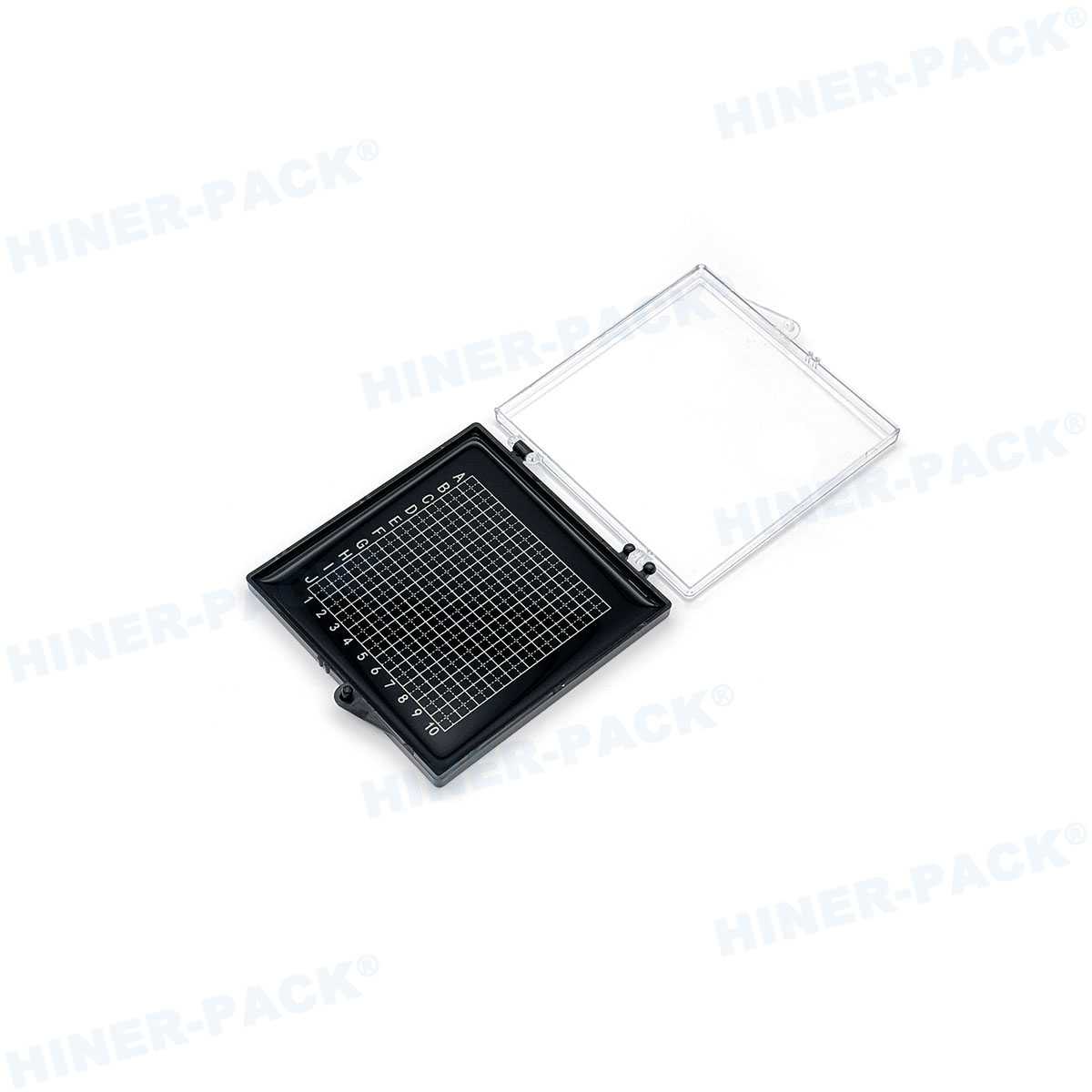
1. The Structural Role of the Wafer Jar in Automated Manufacturing
Modern 300mm fabs operate with over 90% automation, where wafer
jars (FOUPs) are transported by overhead hoist transport (OHT) systems
between process tools. Each wafer jar accommodates 25 wafers,
maintaining a controlled atmosphere with purge ports for nitrogen or clean dry
air (CDA). The interface between the wafer jar and the
equipment front end module (EFEM) involves mechanical docking, door opening, and
wafer mapping—a sequence repeated thousands of times daily. Failures in this
interface—such as misalignment, particle generation during door actuation, or
seal degradation—account for approximately 5–8% of unscheduled tool downtime in
high-volume manufacturing (HVM) lines. Therefore, selecting a wafer
jar requires evaluating mechanical durability (latch cycles), chemical
stability, and cleanroom compatibility.
2. Material Science: Polymer Selection for Particle Control and
Outgassing
2.1 Polycarbonate (PC) vs. Polyetheretherketone (PEEK) vs. Cyclic Olefin
Copolymer (COC)
Historically, wafer jars were manufactured from
polycarbonate due to its optical clarity and low cost. However, polycarbonate
exhibits high moisture absorption (0.15–0.20% at 23°C) and outgassing of
bisphenol A (BPA) and other oligomers, which condense on wafer surfaces and
cause micro-droplet defects during thermal processing. For 7nm and below,
leading fabs have transitioned to wafer jars fabricated from
PEEK or COC blends. PEEK offers superior chemical resistance, lower outgassing
(total mass loss < 0.1% per SEMI E46), and higher mechanical strength,
allowing for longer lifecycle (> 10,000 clean cycles). COC provides the
lowest particle generation during sliding contact, making it preferred for
advanced logic where particle adders must remain below 0.05 particles/cm² for
>0.1 µm.
Recent industry data from a leading equipment manufacturer indicates that
switching from polycarbonate to PEEK-based wafer jars reduced
front-end-of-line (FEOL) defect densities by 22% in a 5nm pilot line,
attributable to lower volatile organic compound (VOC) outgassing and reduced
moisture adsorption.
2.2 Anti-Static and ESD Control
Electrostatic discharge (ESD) events within a wafer jar can
result in charge-induced damage to gate oxides. Modern containers incorporate
static-dissipative additives (e.g., carbon nanotubes or conductive polymers) to
achieve surface resistivity between 10⁶ and 10¹⁰ Ω/sq. Measurement protocols per
ANSI/ESD S20.20 mandate that wafer jars maintain discharge
times under 2 seconds. Failure to meet these specifications has been linked to
1–3% yield loss in sensitive memory devices, particularly during winter months
when humidity drops below 30% in cleanrooms.
3. Contamination Control: Particles, Moisture, and Airborne Molecular
Contaminants (AMCs)
The primary function of a wafer jar is to isolate wafers
from the fab ambient. Three contamination vectors dominate:
Particle Adhesion: Particles between 10–100 nm adhere via
van der Waals forces. The jar's interior surface roughness (Ra < 0.1 µm) and
material hardness directly influence particle detachment during transport. A
study by SEMI found that wafer jars with textured interior
surfaces increased particle adders by a factor of 2.5 compared to smooth-molded
variants.
Moisture Control: In-line moisture sensors within FOUPs
track relative humidity (RH). For EUV lithography processes, wafers must be
maintained below 5% RH to prevent haze formation on reticles and resist
blistering. Advanced wafer jars integrate nitrogen purge
systems that achieve 1–2% RH within 120 seconds after docking.
Airborne Molecular Contaminants (AMCs): Amines, ammonia,
and acid gases from cleanroom materials can adsorb onto wafer surfaces and react
with photoresist. High-performance wafer jars employ chemical
filters (activated carbon and ion-exchange media) in purge ports to reduce AMC
concentrations to below 0.1 ppb for critical process steps.
For companies like Hiner-pack, which
specializes in certified packaging solutions, the emphasis is on pre-cleaned
wafer jars that meet ISO Class 2 cleanroom standards upon
delivery. Their validated cleaning processes ensure that particle counts per jar
remain under 50 particles >0.1 µm, reducing pre-insertion cleaning time for
fab operators.
4. Mechanical Interface and Automation Compatibility
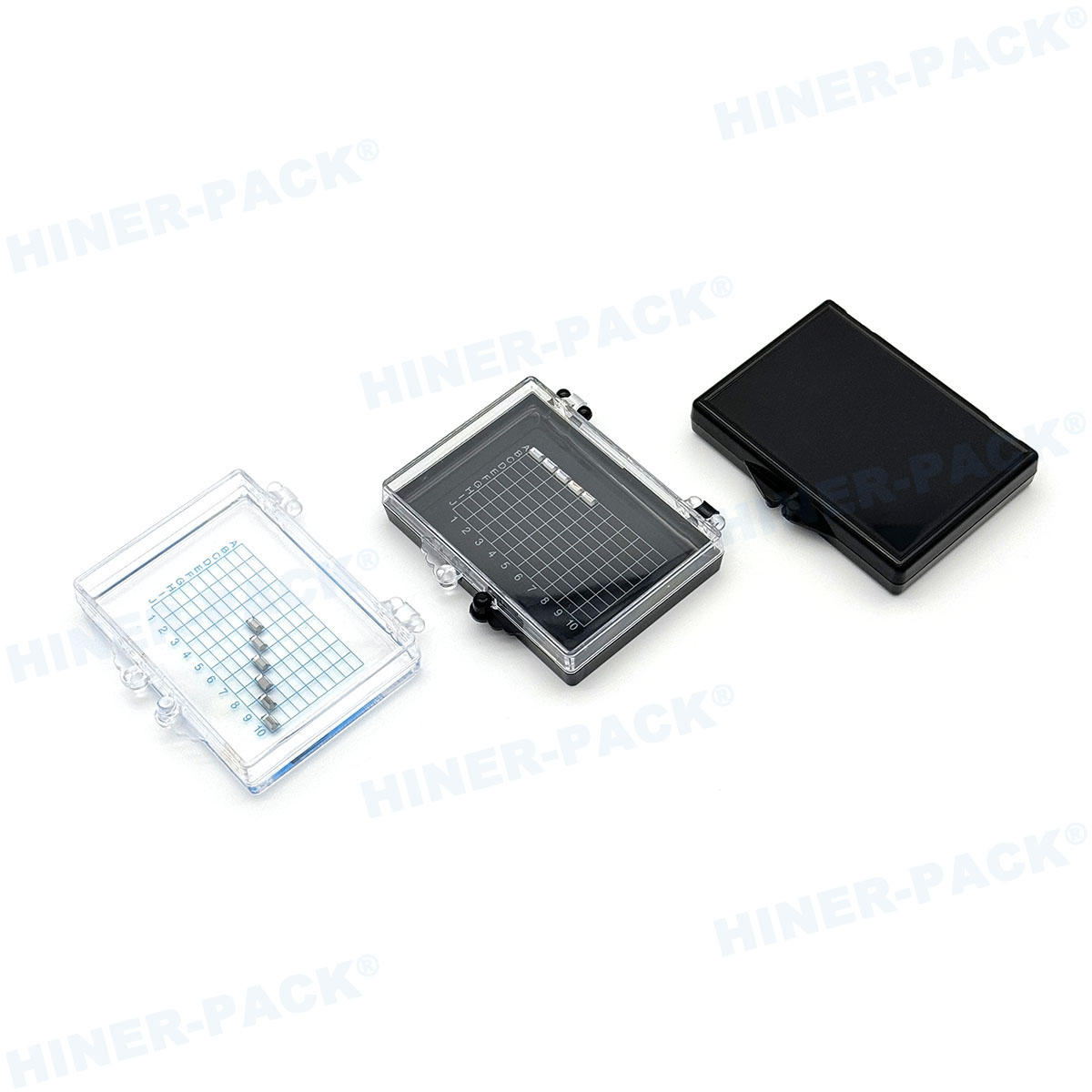
4.1 FOUP vs. FOSB: Operational Distinctions
It is essential to differentiate between FOUPs (used for intra-fab transport)
and FOSBs (used for inter-fab shipping). A FOUP wafer jar features a mechanical kinematic coupling that aligns with tool load ports to a
precision of ±0.1 mm. FOSBs, in contrast, are designed for shock absorption
during shipping, with foam-lined interiors and double-wall construction to
withstand 1-meter drop tests. Mixing these applications leads to premature seal
failure and contamination ingress; FOUPs used in shipping often exceed 50
particle adder counts due to inadequate vibration dampening.
4.2 Latch Mechanism and Door Sealing
The door interface is the most mechanically stressed component of any
wafer jar. A double-lip EPDM or FFKM seal ensures leak
integrity, with leak rates maintained below 0.1 sccm at 1 psi differential
pressure. Over 10,000 open/close cycles, seal compression set can reduce sealing
force by 15%, leading to micro-leaks that allow particle ingress. Predictive
maintenance protocols now track cycle counts per wafer jar via
RFID tags, triggering re-certification when cycle thresholds (typically 7,500
cycles for FOUPs) are approached.
5. Industry Pain Points: Cross-Contamination, Reusability, and
Traceability
5.1 Cross-Contamination from Mixed Products
In foundry environments, the same wafer jar may carry wafers
from multiple customers and process flows. Residual metallic contamination
(e.g., Cu, Ni) left in the jar from previous lots can cross-contaminate
sensitive analog or power device wafers. To mitigate this, advanced fabs enforce
strict jar segregation by technology node and implement non-destructive surface
extraction sampling (e.g., ICP-MS analysis of swabs) to verify cleanliness
before reuse. Data shows that implementing such protocols reduces
contamination-related rework by 18% in multi-product fabs.
5.2 Lifecycle Management and Reclamation
A high-quality wafer jar is designed for 5–10 years of
service with proper reconditioning. Reclamation involves ultrasonic cleaning,
surface resistivity testing, and optical inspection for scratches or
deformation. However, over 30% of jars are prematurely retired due to improper
cleaning agents that cause surface crazing or embrittlement. Standardized
cleaning per SEMI E125 (specifying pH-neutral detergents and deionized water
rinses) can extend jar life by 40%.
5.3 RFID and Digital Traceability
Modern wafer jars are embedded with passive RFID tags that
store lot history, slot maps, and environmental log data. These tags enable
real-time inventory tracking and automated material handling systems to route
jars to the correct process tools. A leading memory manufacturer reported that
implementing RFID-enabled wafer jars reduced misrouted lots by
97% and improved tool utilization by 4% due to faster identification.
6. Cost-Benefit Analysis: Premium Materials vs. Extended Lifespan
While a standard polycarbonate wafer jar costs between $150
and $250, a PEEK-based jar commands $450–$600. However, total cost of ownership
(TCO) models reveal that PEEK jars yield a 35% lower cost per wafer pass due to
reduced cleaning frequency (every 12 months vs. 6 months for PC) and lower
particle adder-related yield loss. For a 50,000 wafer starts per month (WSPM)
fab, switching to high-performance wafer jars yields an
estimated $2.8M annual savings from yield improvement alone, making the upfront
material premium negligible in the context of overall profitability.
Hiner-pack leverages this TCO analysis to offer tiered
product lines—from certified reclaimed jars for non-critical layers to
high-purity, ultra-low outgassing jars for EUV and gate-all-around (GAA)
processes—allowing customers to match jar performance to process risk
tolerance.
7. Future Developments: 450mm Transition, E-Scanning, and Smart Jars
Although the 450mm wafer transition has slowed, the need for larger
wafer jars persists for advanced packaging and panel-level
processing. Prototype 450mm FOUPs weigh over 12 kg when loaded, necessitating
new materials with higher strength-to-weight ratios, such as
carbon-fiber-reinforced polymers. Additionally, the industry is moving toward
“smart jars” equipped with embedded sensors for continuous monitoring of
humidity, particle counts, and shock events. These smart wafer
jars transmit data via IoT gateways to fab MES systems, enabling
predictive cleaning schedules and real-time lot release decisions. Early
adopters report a 60% reduction in excursions caused by out-of-spec storage
conditions.
The Wafer Jar as a Yield Enabler, Not Just a Container
For semiconductor manufacturing professionals, the wafer jar represents a critical control point that directly influences defect density,
equipment uptime, and logistics efficiency. The evolution from simple storage
box to engineered microenvironment demands rigorous attention to material
science, contamination control, and automation compatibility. As device
geometries continue to shrink and process complexity increases, the strategic
selection and management of wafer jars will remain a
cornerstone of operational excellence. Companies that invest in advanced jar
technologies and disciplined lifecycle management will secure measurable
advantages in yield and cost competitiveness.
Frequently Asked Questions (FAQs)
Q1: What is the primary difference between a FOUP and a FOSB in wafer
jar terminology?
A1: A FOUP (Front Opening Unified Pod) is a
wafer jar designed for automated intra-fab transport, featuring
a kinematic coupling for precise tool alignment and nitrogen purge capabilities.
A FOSB (Front Opening Shipping Box) is intended for inter-fab or cross-site
shipping, with reinforced shock absorption and double-wall construction to
withstand transportation vibrations. Using a FOUP for shipping voids its
contamination control performance and accelerates mechanical wear.
Q2: How often should a wafer jar be cleaned, and what standards
apply?
A2: Cleaning frequency depends on process node and
contamination history. For leading-edge logic (<7nm), wafer
jars are typically cleaned every 6–12 months or after 1,500 lot passes.
Cleaning must comply with SEMI E125 for particle removal and SEMI E46 for
outgassing verification. The process involves multi-stage ultrasonic cleaning
with deionized water, followed by Class 1 cleanroom drying and surface
resistivity testing to confirm ESD performance remains within specification.
Q3: What causes particle generation from a wafer jar, and how is it
measured?
A3: Particle generation originates from three main
sources: mechanical abrasion during door opening, static discharge attracting
airborne particles, and material shedding from jar walls. Measurement follows
SEMI E127, where the jar is subjected to 100 opening cycles in a cleanroom, and
particle counts on a test wafer are measured using a surface scanner. Acceptance
criteria for advanced nodes require <0.05 added particles per cm² for >0.1
µm particles.
Q4: Can wafer jars be recycled or repaired after reaching their
lifecycle limit?
A4: Yes, wafer jars can undergo
recertification involving replacement of seals, RFID tags, and latch mechanisms,
followed by full requalification testing. However, if the jar body exhibits
crazing, warpage (>1 mm over 300 mm), or surface resistivity deviation beyond
±2 decades, it must be retired. Some suppliers, including Hiner-pack, offer trade-in programs where retired jars
are recycled into raw polymer materials, supporting sustainability goals in
semiconductor supply chains.
Q5: How does moisture control inside a wafer jar impact
photolithography processes?
A5: High humidity (>10% RH) within a
wafer jar can cause moisture absorption in photoresist layers,
leading to line edge roughness (LER) and pattern collapse in high aspect ratio
features. For immersion lithography and EUV, moisture also interacts with the
resist surface to form watermarks that become printable defects. Advanced jars
incorporate active purge systems that maintain <2% RH using nitrogen flow
rates of 50–100 L/min, ensuring wafer stability during queuing times.
Q6: What role does Hiner-pack play in the wafer jar supply
chain?
A6: Hiner-pack provides
certified, pre-cleaned wafer jars with validated particle and
AMC levels, along with RFID-enabled tracking systems. Their logistics platform
offers just-in-time delivery, bar-coded traceability, and compliance
documentation for SEMI standards, reducing the burden on fabs to qualify and
maintain jar inventories internally.


