In semiconductor manufacturing, MEMS fabrication, and advanced
optoelectronics, the physical protection of delicate devices during transport,
dicing, and assembly is critical. Standard trays or tape‑and‑reel often cannot
provide the necessary shock absorption or contamination control. Custom gel pak
solutions address these challenges by combining a soft, compliant gel
layer with precisely machined cavities to immobilize and cushion individual
components. This article explores the materials science, design parameters, and
application‑specific engineering of custom gel pak systems, with insights from
Hiner‑pack, a leader in
precision wafer and chip packaging.
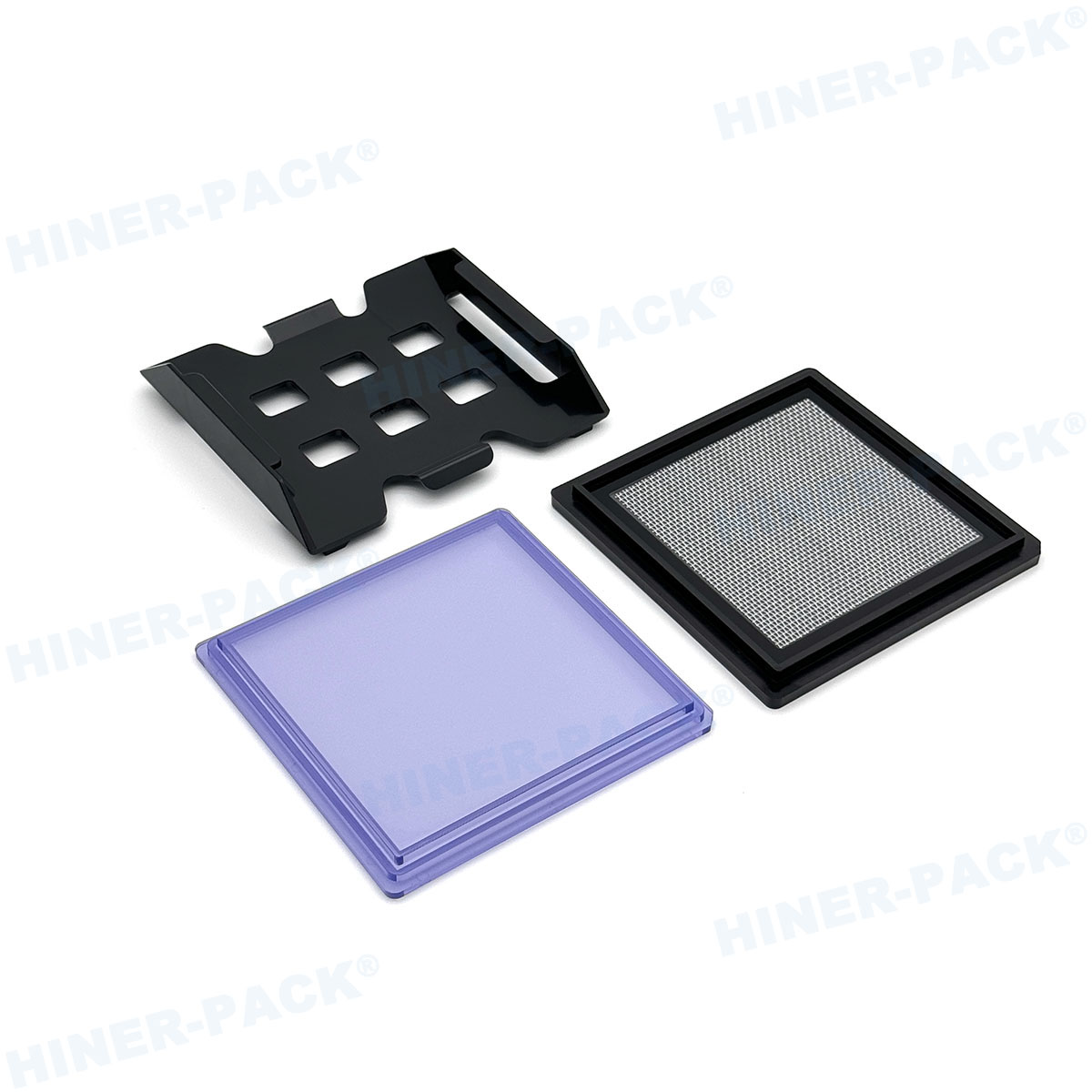
Fundamentals of gel pak technology
Gel pak carriers consist of a low‑modulus, viscoelastic gel membrane bonded
to a rigid substrate (typically plastic or metal). The gel’s tackiness and
conformability allow it to gently hold components in place, while its ability to
flow under pressure provides excellent shock damping. When the gel is
vacuum‑released, it loses tack, enabling non‑contact removal of even the most
fragile devices.
Gel chemistry and properties
The gel is typically a silicone‑based or polyurethane material formulated to
achieve specific durometer (hardness), tack level, and outgassing
characteristics. For semiconductor applications, low outgassing (low total mass
loss, low collected condensables) is essential to prevent contamination of
sensitive surfaces. Gel formulations can be tailored to meet NASA ASTM E595 or
ISO 14644 cleanliness standards. Thermal stability from –40 °C to +150 °C is
often required for processes that include baking or cold shipping.
Vacuum release mechanism
A key differentiator of custom gel pak
solutions is the ability to temporarily eliminate tack via vacuum. A
porous support beneath the gel allows air to be drawn through, pulling the gel
away from the component and releasing it without mechanical force. This is
critical for thin, brittle dies (e.g., GaAs, InP) or MEMS structures with moving
parts.
Design parameters for custom gel pak solutions
Effective custom gel pak
solutions are not off‑the‑shelf products; they are engineered around the
specific device and process flow. Key design variables include:
Cavity geometry – Pockets can be machined, etched, or
molded to match component dimensions. Tolerances as tight as ±0.05 mm ensure
precise positioning for pick‑and‑place equipment.
Gel thickness and hardness – Thicker, softer gels (e.g., 30
Shore 00) provide maximum shock absorption for fragile devices, while firmer
gels (60 Shore 00) offer better positional stability for heavy components.
Tack level – Adjustable via formulation. Low‑tack gels are
used for devices with fragile coatings; higher tack ensures retention during
shipping.
Carrier material – Options include static‑dissipative
plastics (surface resistivity 10⁶–10⁹ Ω/sq), aluminum, or stainless steel for
cleanroom compatibility and ESD safety.
Frame format – JEDEC trays, 2‑inch to 12‑inch rings, or
custom magazine formats to fit automated handlers.
Hiner‑pack collaborates with
customers to define these parameters, often creating prototypes for process
validation before volume production.
Applications across the semiconductor ecosystem
Custom gel pak
solutions are deployed in multiple stages of device fabrication and
assembly.
Die handling after dicing
After wafer dicing, individual dies are often transferred to gel paks for
transport to die attach or test. The gel holds dies securely but releases them
cleanly under vacuum, eliminating the need for ejector pins that can crack thin
dies. This is particularly valuable for stacked‑die assemblies and memory
chips.
MEMS and sensor packaging
Micro‑electromechanical systems (MEMS) contain fragile cantilevers,
membranes, or inertial structures. Standard pick‑and‑place can damage these. Gel
paks immobilize the entire device without contacting sensitive areas, and vacuum
release ensures no force is applied during removal. Accelerometers, gyroscopes,
and pressure sensors are routinely shipped in custom gel trays.
Optoelectronic components
Laser diodes, photodetectors, and fiber‑optic assemblies require scratch‑free
surfaces and precise alignment. Custom gel pak
solutions with individual cavities prevent device‑to‑device contact and
provide ESD protection. Some designs incorporate alignment pins for direct
placement into test fixtures.
Known good die (KGD) and bare die inventory
Semiconductor manufacturers often stock bare dies for multichip modules. Gel
paks allow long‑term storage without die attach tape residue, and the gel’s
chemical inertness prevents corrosion. Vacuum sealing in moisture‑barrier bags
extends shelf life.
Process challenges and technical solutions
Implementing custom gel pak
solutions requires addressing several engineering challenges.
Particle and ionic contamination
Gel materials must be ultra‑pure. Hiner‑pack uses formulations with low
extractable ions (Na⁺, K⁺, Cl⁻ below 10 ppb) and no migratory plasticizers.
Cleanroom manufacturing (Class 100 or better) and double‑bagging ensure that
delivered trays meet the most stringent fab requirements.
ESD control
Many semiconductor devices are sensitive to electrostatic discharge. Gel paks
are available with static‑dissipative properties (surface resistivity
10⁶–10⁹ Ω/sq) throughout the gel and carrier, complying with ANSI/ESD S20.20.
Some designs incorporate conductive carbon or embedded fibers.
Thermal cycling and outgassing
Devices may undergo thermal cycling while in the gel pak (e.g., burn‑in). Gel
formulations must remain stable without melting, excessive softening, or
outgassing that could fog optical surfaces. Hiner‑pack provides TGA
(thermogravimetric analysis) data and outgassing profiles per ASTM E595 for
customer qualification.
Automated handling compatibility
High‑volume assembly uses automated pick‑and‑place machines. Gel trays must
maintain precise x‑y location of each die (typically ±0.1 mm) and present a flat
surface for vision systems. Custom gel pak solutions can include alignment
features or barcode areas for traceability.
Engineering workflow for custom gel paks
A structured approach ensures that custom gel pak
solutions meet all technical and operational requirements.
Device characterization – Dimensions, weight, fragility
(e.g., break force), surface sensitivity, and ESD class are documented.
Process mapping – How will the gel pak be used? Manual or
automated pick‑and‑place? Will it undergo vacuum release? Is there a baking
step?
Gel selection – Based on tack, durometer, and thermal
requirements. Prototype gels are tested for compatibility with device materials
(no adhesion or residue).
Cavity design – CAD modeling of pocket geometry, including
draft angles for easy insertion. Tolerance analysis ensures fit across device
lot variations.
Tooling and prototyping – CNC‑machined or molded prototypes
are produced and tested with actual devices. Pick‑and‑place trials verify
release and placement accuracy.
Validation – Outgassing, ionic cleanliness, and mechanical
shock/drop tests are performed. Data is shared with the customer for
qualification.
Volume production – Quality control includes 100% visual
inspection and statistical sampling of gel integrity.
Hiner‑pack offers this full
engineering service, with typical lead times of 2–4 weeks for prototypes.

Quality and compliance standards
Reputable custom gel pak
solutions adhere to international standards:
ISO 14644‑1 – Cleanroom manufacturing environment (Class 7
or better).
ASTM E595 – Outgassing testing (TML ≤ 1.0%, CVCM ≤ 0.1%
typically).
ANSI/ESD S20.20 – ESD control program compliance.
RoHS / REACH – Restriction of hazardous substances.
JEDEC J‑STD‑020 – Moisture sensitivity level (MSL)
compatibility for storage.
Hiner‑pack provides
certificates of compliance and full material disclosure upon request.
Frequently asked questions about custom gel pak solutions
Q1: What types of devices are best suited for gel pak
packaging?
A1: Gel paks are ideal for fragile, thin, or small
devices that cannot tolerate mechanical stress. Common examples include bare
semiconductor dies, MEMS sensors, laser diodes, photonic chips, and hybrid
microcircuits. They are also used for components with delicate coatings or air
bridges.
Q2: How does vacuum release work, and is it compatible with all
pick‑and‑place machines?
A2: A porous substrate beneath the gel
allows vacuum to be drawn from below, pulling the gel away from the component.
The device then sits loosely in the cavity and can be lifted with standard
vacuum tweezers or pick‑and‑place collets. Many machines can be programmed to
activate a vacuum pulse just before picking. Hiner‑pack offers trays with
integrated vacuum ports for seamless automation.
Q3: Can gel paks be used in high‑temperature processes like die
attach curing?
A3: Yes, but the gel formulation must be selected for
the specific temperature range. Standard silicone gels handle continuous use up
to 150 °C. For higher temperatures (e.g., 200 °C), specialty high‑temperature
gels are available. Always verify outgassing at process temperature to avoid
contamination.
Q4: How do I prevent devices from sticking permanently to the
gel?
A4: Sticking can occur if the gel is too tacky for the device’s
surface or if the device remains in contact for extended periods under pressure.
Solutions include: reducing gel tack (formulation adjustment), using a low‑tack
“release” gel, or ensuring that vacuum release is applied before removal. Hiner‑pack engineers can recommend
the appropriate tack level based on device weight and surface material.
Q5: Are custom gel pak solutions reusable?
A5: Most gel
paks are designed for single‑use to guarantee cleanliness and tack consistency.
However, some heavier‑duty trays can be reused if they are not contaminated and
the gel retains its properties. Reusable trays require careful cleaning and
validation. For critical semiconductor applications, single‑use is strongly
recommended to avoid cross‑contamination.
Q6: What is the typical lead time for a custom
design?
A6: For standard cavity arrays on common formats (e.g.,
4‑inch ring, JEDEC tray), prototypes can be delivered in 2–3 weeks. Complex
multi‑cavity designs or special carrier materials may require 4–6 weeks. Hiner‑pack offers expedited services
for urgent development programs.
Q7: How do I specify a custom gel pak for my device?
A7:
Provide device drawings (or samples), describe the process flow (manual vs.
automated, vacuum release needed, temperature exposure), and indicate any
special requirements (ESD, outgassing limits). Our engineers will then propose
gel type, cavity geometry, and carrier format. A formal specification document
is created for approval before tooling.