In semiconductor fabs and back-end assembly plants, the safe and
contamination‑free transport of silicon wafers is paramount. Among the various
materials used for wafer carriers, polypropylene (PP) has emerged as a preferred
choice due to its excellent chemical resistance, low particle shedding, and
cost‑effectiveness. PP wafer
carriers are widely employed for in‑process storage, inter‑facility
shipping, and equipment interfacing. This article provides a comprehensive
technical overview of PP wafer carriers, including material science, design
considerations, application scenarios, and how suppliers like Hiner‑pack engineer carriers to meet
the stringent demands of modern semiconductor manufacturing.
Polypropylene as a wafer carrier material
Polypropylene is a thermoplastic polymer known for its semi‑crystalline
structure, which imparts a unique combination of mechanical strength and
chemical inertness. For wafer handling, several grades are used:
Homopolymer PP – High stiffness and good chemical
resistance, suitable for carriers that require dimensional stability at elevated
temperatures (up to 120 °C).
Copolymer PP – Enhanced impact resistance, often used for
shipping boxes that may experience mechanical shock.
Carbon‑filled conductive PP – Provides static dissipation
(surface resistivity 10⁶–10⁹ Ω/sq) to protect ESD‑sensitive devices.
All grades used for PP wafer
carriers must meet strict purity requirements: low ionic extractables
(Na⁺, K⁺, Cl⁻ below 10 ppb), minimal outgassing, and no migratory additives.
Hiner‑pack sources only virgin,
FDA‑grade resins to ensure batch‑to‑batch consistency.
Key material properties
Chemical resistance – PP withstands acids, alkalis, and
many organic solvents, allowing carriers to be cleaned with aggressive agents
without degradation.
Low particle generation – Properly molded PP exhibits low
friction and does not flake, critical for maintaining cleanroom Class 1 or ISO 3
environments.
Thermal stability – PP maintains its shape up to 120 °C,
enabling carriers to be used in processes like wafer baking or autoclave
sterilization.
Light weight – Density of ~0.9 g/cm³ reduces operator
fatigue and shipping costs.
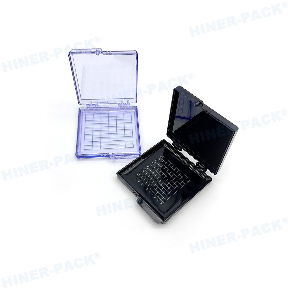
Types of PP wafer carriers
PP wafer
carriers are available in multiple formats to suit different handling
requirements.
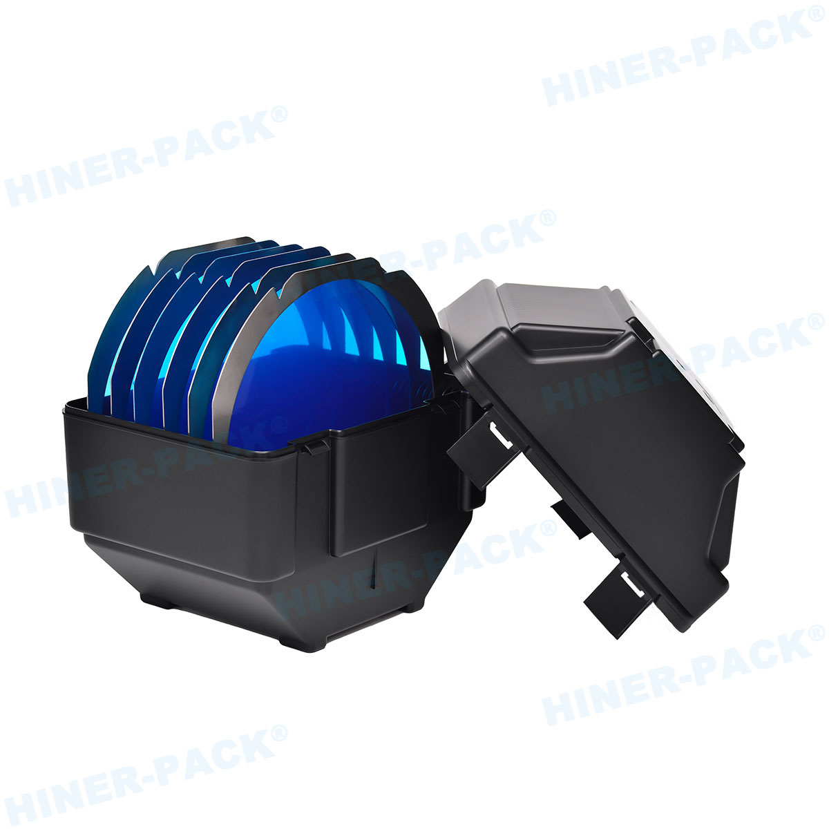
Wafer shipping boxes
These are closed containers designed to protect wafers during transport. They
typically feature:
Cushioned inserts (often conductive foam or gel) to absorb shock.
Tamper‑evident seals and moisture‑barrier bags for long‑term storage.
Stackable designs for efficient palletization.
Shipping boxes must pass ISTA or ASTM drop test standards to ensure wafer
integrity.
Wafer racks and carriers for wet processing
In wet etch or cleaning stations, carriers hold wafers vertically while
allowing fluid flow. PP’s chemical resistance makes it ideal for these
applications. Carriers are designed with minimum contact to the wafer edge,
often using knife‑edge supports to reduce contamination.
FOUP and FOSB alternatives
While front‑opening unified pods (FOUPs) for 300 mm wafers are typically made
of polycarbonate, some specialty applications use PP for its lower cost or
specific chemical compatibility. PP is also used for 200 mm and smaller wafer
carriers in less automated lines.
Open cassettes and boats
For manual handling or furnace operations, open‑slot carriers (boats) made of
PP hold wafers securely. Precision molding ensures consistent slot pitch
(typically 4.76 mm or 6.35 mm) to prevent wafer binding.
Design criteria for high‑performance PP wafer carriers
Engineering effective PP wafer
carriers requires attention to multiple factors.
Dimensional tolerance and stability
Wafer carriers must maintain critical dimensions (e.g., slot width, overall
flatness) within ±0.1 mm to ensure compatibility with automated handling
equipment. PP’s coefficient of thermal expansion (CTE) is ~100 ppm/°C, so
designs must account for temperature variations in the fab. Hiner‑pack uses finite element
analysis (FEA) to predict dimensional changes and optimizes gate locations in
molds to minimize warpage.
Cleanroom compatibility
Carriers molded in Class 100 cleanrooms undergo post‑mold cleaning (e.g.,
deionized water rinse, HEPA‑filtered air blow‑off) to remove any residual
particles. Materials are selected to avoid outgassing that could fog optics or
contaminate sensitive layers. Surface smoothness (Ra < 0.5 µm) reduces
particle adhesion.
ESD control
For devices vulnerable to electrostatic discharge, conductive or
static‑dissipative PP grades are used. These maintain surface resistivity
between 10⁶ and 10⁹ Ω/sq, even after repeated cleaning cycles. Grounding
features (e.g., contact points) can be integrated into the carrier design.
Automated handling interface
Carriers used with robotic handlers require precise alignment features, such
as kinematic coupling grooves or RFID tag pockets. Gripper clearance areas and
weight limits must be considered. Hiner‑pack designs carriers that meet
SEMI E47.1 and other industry standards for equipment interfacing.
Applications across the semiconductor lifecycle
PP wafer
carriers are deployed in multiple stages of wafer processing and
handling.
Wafer fabrication (front‑end)
In fabs, carriers are used to move wafers between tools, particularly in less
automated legacy lines or for engineering runs. They protect wafers from
mechanical damage and airborne particles during manual transport.
Metrology and inspection
Wafers are often placed in carriers for transport to metrology tools. The
carrier must hold wafers securely without obscuring the edge or backside, where
measurements may be taken. Open‑frame designs allow access.
Wafer bumping and thinning (back‑end)
During bumping, thinning, or dicing, wafers are fragile and require careful
handling. PP carriers with cushioning features protect the device side while
allowing access to the backside for grinding or etching.
Shipping of bare or processed wafers
For outsourcing or internal transfers, shipping boxes made of PP provide
mechanical protection and a controlled atmosphere. Gel or foam liners cushion
wafers, while ESD‑safe materials prevent charge accumulation.
Process challenges and solutions
Implementing PP wafer
carriers successfully requires addressing common operational issues.
Particle contamination
Even clean‑molded carriers can accumulate particles from the environment.
Regular cleaning in automated washers using deionized water and non‑ionic
surfactants is recommended. Hiner‑pack provides cleaning
validation protocols and recommends intervals based on fab particle counts.
Chemical attack from aggressive processes
While PP resists many chemicals, some concentrated acids or solvents (e.g.,
sulfuric acid, hydrogen peroxide mixtures) can cause stress cracking over time.
Material selection should match the specific chemistry of the process. For harsh
environments, special PP grades with enhanced chemical resistance are
available.
Warpage after high‑temperature exposure
Carriers used in baking steps may warp if not properly annealed. Post‑mold
annealing (e.g., 100 °C for 2 hours) relieves internal stresses. Hiner‑pack offers annealed carriers
for applications requiring thermal stability.
ESD degradation over time
Conductive additives can migrate to the surface or be worn away by repeated
handling. Periodic resistivity testing ensures carriers remain within
specification. Dissipative carriers typically have a service life of 2–5 years
depending on usage.
Quality and compliance standards
Reputable PP wafer
carriers adhere to industry standards:
SEMI M31 – Specifications for wafer carriers and shipping
boxes.
SEMI E47.1 – Kinematic coupling interface for 300 mm
carriers.
ISO 14644‑1 – Cleanroom manufacturing environment
(typically Class 7 or better).
ANSI/ESD S20.20 – ESD control program compliance.
RoHS / REACH – Restriction of hazardous
substances.
Hiner‑pack provides
certificates of analysis for material purity and dimensional inspection reports
upon request.
Frequently asked questions about PP wafer carriers
Q1: What is the maximum temperature PP wafer carriers can
withstand?
A1: Standard polypropylene can be used continuously up to
120 °C. For short periods (e.g., autoclaving), temperatures up to 130 °C are
possible, but repeated cycles may cause deformation. Always verify with the
manufacturer’s data sheet. Hiner‑pack offers high‑temperature PP
grades for applications up to 140 °C.
Q2: Can PP wafer carriers be used in wet chemical
processes?
A2: Yes, PP is resistant to most acids, bases, and
aqueous solutions used in semiconductor wet processing. However, strong
oxidizing agents (e.g., hot sulfuric acid with peroxide) may cause degradation
over time. For such chemistries, consider PTFE or PFA carriers. Hiner‑pack can advise on chemical
compatibility based on your specific process.
Q3: How do I clean PP wafer carriers without damaging
them?
A3: Automated wafer carrier cleaners using deionized water and
non‑ionic surfactants are recommended. Avoid abrasive brushes that could roughen
the surface. Ultrasonic cleaning is effective for particle removal. After
cleaning, rinse thoroughly and dry in a HEPA‑filtered environment. Hiner‑pack provides detailed cleaning
protocols.
Q4: Are PP wafer carriers ESD‑safe by default?
A4:
Standard polypropylene is an insulator and can generate static charge. For ESD
protection, carriers must be made from conductive or static‑dissipative PP
compounds. These are typically black or gray in color due to the carbon filler.
Specify “ESD‑safe” when ordering. PP wafer
carriers from Hiner‑pack are available in both
standard and ESD‑safe versions.
Q5: What is the typical lifespan of a PP wafer
carrier?
A5: With proper cleaning and handling, PP carriers can last
3–5 years in a production environment. Factors that reduce lifespan include:
exposure to UV light (causes embrittlement), repeated high‑temperature cycling,
and mechanical impacts. Regular inspection for cracks, warpage, or discoloration
is recommended.
Q6: Can PP wafer carriers be recycled?
A6: Yes,
polypropylene is recyclable. Many semiconductor suppliers offer take‑back
programs for end‑of‑life carriers. Hiner‑pack participates in recycling
initiatives and can advise on proper disposal.
Q7: How do I specify a custom PP wafer carrier for non‑standard wafer
sizes?
A7: Provide the wafer diameter, thickness, and any special
requirements (e.g., notch location, flat orientation, handling automation). Our
engineers will design a carrier with appropriate slot pitch, support geometry,
and material selection. Prototypes can be delivered in 3–4 weeks for
validation.


