Dual In-line Packages (DIP) remain widely deployed in industrial controllers,
automotive modules, and legacy systems where through-hole assembly offers
superior mechanical bonding. Unlike surface-mount devices, DIP components
feature fragile leads that demand careful handling, coplanarity control, and
anti-static protection across test, burn-in, and PCB assembly lines. The
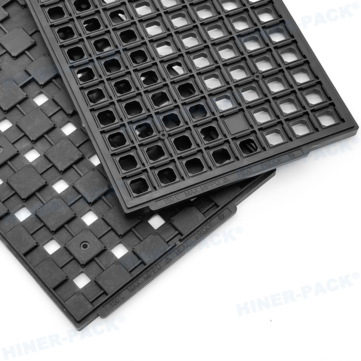
standardized solution for high-volume DIP logistics is the DIP JEDEC
matrix IC trays. These precision-molded trays combine JEDEC global
standards with lead-pocket geometry specifically adapted for DIP body sizes and
pin arrays. This guide provides engineering deep-dive into tray design, material
performance, and operational workflows, drawing on semiconductor back-end
expertise to help process engineers reduce lead damage and improve
throughput.
1. JEDEC Standards for DIP Trays: Matrix Layouts, Cell Geometry, and Stack
Interoperability
The JEDEC Solid State Technology Association specification
JESD95-1 defines outline dimensions, cell pitch, and stack
profiles for DIP JEDEC
matrix IC trays. Typical tray outlines include 322 mm × 322 mm
(large matrix) and 196 mm × 245 mm (miniature) to fit automatic tray feeders.
The matrix arrangement, commonly 5×18, 6×24, or 8×28 cells, aligns with DIP body
widths of 300 mil, 400 mil, or 600 mil.
Key geometric features engineered for DIP packages:
Lead pocket channels: Recessed grooves that support DIP
leads along their length, preventing sideways bending and lead sweep during
transportation.
Center support ribs: Raised pads under the DIP body to
reduce stress on the mold compound while allowing lead tips to remain free from
contact with the tray floor.
Orientation keys: Asymmetric corner features that ensure
consistent device orientation (pin 1 indicator) for automated placement into
aging sockets or wave soldering pallets.
Stacking posts and anti-nesting bumps: Maintain vertical
alignment when stacking up to 30 trays, eliminating lead crush from uneven
compression.
Dimensional tolerances for cell length/width are held to ±0.08 mm, ensuring
that DIP leads do not bind in the cell during pick-and-place operations. The
matrix cell pitch is typically 15 mm to 22 mm, accommodating standard DIP-8
through DIP-48 devices.
DIP leads are susceptible to corrosion, static discharge, and mechanical
deformation. DIP JEDEC
matrix IC trays must provide consistent surface resistivity,
mechanical strength, and thermal stability. The industry relies on three
material classes:
High-temperature Polyetherimide (PEI) with carbon fiber
reinforcement: Offers surface resistance 10⁴–10⁹ Ω/sq, continuous
service up to 180°C, and exceptional flexural modulus (14 GPa) – critical for
supporting heavy DIP devices during burn-in board loading.
Polyphenylene Sulfide (PPS): Withstands 200°C for post-mold
curing and lead-free soldering processes. Low moisture absorption (<0.05%)
prevents dimensional changes in humid production floors.
Static-dissipative Polycarbonate (PC) blends: Cost-effective for ambient test and shipping but limited to 120°C. Suitable for
DIP handling that does not involve high-temperature exposure.
Additionally, the tray material must exhibit low outgassing per ASTM E595 to
avoid lead oxidation from volatile compounds. Hiner-pack provides full
material certification, including outgassing reports and surface resistivity
mapping across the tray matrix. For burn-in applications up to 150°C, Hiner-pack offers
PEI-based DIP JEDEC trays with reinforced corners to prevent warpage during
72-hour thermal cycling.
3. Application Scenarios: From IC Testing to Through-Hole Assembly
Lines
3.1 High-Temperature Burn-In and Dynamic Aging
DIP devices for automotive and military applications require burn-in at
125°C–150°C for 96 to 168 hours. Trays must maintain flatness (<0.6 mm
overall warpage) to ensure DIP leads align with zero-insertion-force (ZIF)
sockets. Matrix trays with machined guide slots absorb thermal expansion
differences between plastic DIP bodies and the tray matrix.
3.2 Automated IC Handling and Tape & Reel Transfer
Leading OSATs use vacuum pick-and-place
compatible tray nests to transfer DIPs from matrix trays into tube
feeders or tape-on-reel systems. The tray cell design must provide a clearance
of 0.5 mm around each DIP lead tip for nozzle access without collision. Hiner-pack builds custom
lead-pocket chamfers that reduce nozzle deflection by 35%.
3.3 In-Process Logistics for Wave Soldering
In board assembly, DIPs are often removed from trays and loaded into wave
solder pallets. The JEDEC matrix tray's stack alignment (centering pins and side
rail recesses) enables direct feeding to palletizers, cutting changeover time by
45% compared to loose tube handling.
4. Critical Industry Pain Points and Solutions for DIP Tray
Applications
Despite mature standards, DIP packaging lines face persistent challenges that
affect yield and lead integrity:
Lead coplanarity loss during tray stacking: Over-stacking
or bent trays cause leads to deform. The solution is reinforced stacking
ribs with a maximum stack height guide (25 trays) and peripheral
steel-reinforced edges for heavy DIP-64 devices.
Triboelectric charging during high-speed conveyor transfer: DIP leads sliding against tray pockets generate voltages above 1 kV, risking
latent ESD damage. Using dissipative trays (surface resistance 10⁶–10⁹ Ω) and
anti-static additives eliminates charge accumulation.
Contamination from recycled trays: Reused trays accumulate
solder flux residues and particles >0.3 µm on lead surfaces. A closed-loop
cleaning protocol (ultrasonic DI water + 60°C drying) combined with particle count
verification restores Class 1000 cleanliness.
Thermal mismatch with burn-in board sockets: If the tray
coefficient of thermal expansion (CTE) differs from DIP leads, lead binding
occurs. Specifying trays with CTE < 25 ppm/°C (e.g., glass-filled PEI)
resolves insertion/withdrawal problems.
By implementing these engineered fixes, manufacturers reduce DIP lead repair
rates by up to 55% and improve first-pass test yields.
5. Engineering Selection Guide: Specifying DIP JEDEC
matrix IC trays for Production Environments
Procurement engineers must evaluate five critical parameters when selecting
DIP trays:
JEDEC Outline Code: Verify tray size (e.g., Tray-322-25 or
T-240-16) matches automated handlers. Check cell matrix (X×Y) against DIP body
width and pin count.
Lead pocket depth and lead clearance: Pocket must
accommodate lead length (typically 3.4 mm to 4.2 mm) without forcing lead tips
against the tray floor. Minimum clearance = 0.2 mm for thermal expansion.
Temperature rating: For burn-in above 125°C, select PPS or
PEI materials. For shipping and storage only, PC is acceptable.
ESD classification: Per ANSI/ESD STM11.11, require surface
resistance < 1×10¹¹ Ω. For automated assembly lines, target 10⁶–10⁹ Ω.
Automation features: Look for edge grip slots, fiducial
marks for vision systems, and side notches for tray de-stackers.
Hiner-pack provides an online selection matrix that matches JEDEC tray parameters to
specific DIP body sizes and handling equipment, ensuring seamless integration
without tooling changes.
6. Best Practices for Storage, Cleaning, and Lifecycle Management of DIP
JEDEC Trays
To maximize tray reuse and maintain consistent performance across thousands
of cycles:
Storage environment: Keep trays in original ESD shielding
bags at 15°C–30°C, 30–60% RH. Avoid direct sunlight or UV exposure which
degrades dissipative additives.
Cleaning procedure: Use automated tray washers with
deionized water and mild alkaline detergent (pH 7.5–8.5) at ≤50°C. Rinse and dry
with HEPA-filtered hot air (≤70°C). Never use abrasive brushes on lead
pockets.
Inspection frequency: After every 100 cycles, measure tray
flatness with a granite plate and dial gauge. Reject trays with warpage > 0.7
mm or cracked cell walls.
Recycling partnership: Participate in take-back programs
that grind and reprocess trays into industrial-grade plastics, reducing waste by
80% and lowering carbon footprint per tray.
7. Frequently Asked Questions (Technical & Operational)
Q1: Can standard DIP JEDEC matrix IC trays withstand repeated exposure to
wave solder flux and cleaning solvents?
A1: Standard trays made of PC or ABS are not chemically
resistant to aggressive flux removers (e.g., isopropyl alcohol, terpenes). For
in-line wave soldering applications where trays enter fluxing zones, specify
chemically resistant PPS or PEI trays. Hiner-pack offers a
chemical compatibility chart for all tray materials. For most logistics-only
applications, keep trays away from soldering areas.
Q2: How do I verify that a tray complies with JEDEC standard MS-001 for DIP
outlines?
A2: Request a JEDEC compliance certificate from the
manufacturer. Key metrics include cell pitch tolerance (±0.05 mm), tray flatness
(≤0.6 mm over 300 mm), and material identification. The tray body should be
stamped with “JEDEC MS-xxx” reference. You can also measure pocket dimensions
using an optical comparator against JEDEC Publication 95 drawings.
Q3: What is the typical cost range for custom vs. standard DIP JEDEC matrix
trays in volumes of 30,000 pieces?
A3: Standard catalog DIP trays (existing matrix size and
cell geometry) cost $0.80–$1.50 per unit at 30k volume. Custom trays (new matrix
pitch, special lead pocket profiles) range from $2.00 to $4.20 per unit,
including initial tooling amortized over 100k pieces. Hiner-pack provides
tooling-sharing programs to reduce custom costs by 30%.
Q4: How many production cycles can a DIP JEDEC matrix IC tray deliver before
performance degrades?
A4: Under normal handling (ESD-safe, no extreme
temperatures, flat stack storage), polycarbonate trays provide 300–500 cycles.
PPS and PEI trays exceed 1,200 cycles. Degradation indicators: surface
resistivity >10¹² Ω, visible pocket wear, or warpage beyond 0.7 mm. Periodic
testing with a surface resistance meter extends reliable use.
Q5: Are there dedicated trays for DIP devices with copper leads (soft lead
finish) to prevent scratching?
A5: Yes. Soft copper leads require tray pockets with smooth,
polished surfaces – no sharp demolding witness lines. Many suppliers offer
nickel-plated mold cavities or special low-friction additives (PTFE) in the tray
resin. Specify “soft-lead friendly” trays and request a lead drag test report.
Hiner-pack's advanced
molding process ensures a surface roughness Ra ≤0.8 µm on all lead
contact areas.
8. Future Directions: Traceable Trays and Smart Logistics for DIP
Packaging
The next generation of DIP JEDEC
matrix IC trays will incorporate molded RFID inlays and conductive
trace patterns that connect to automated storage and retrieval systems (AS/RS).
These smart trays record time-stamped temperature, humidity, and shock events,
directly integrating with quality management software (e.g., MES). For
high-reliability sectors such as aerospace, smart trays trigger preventive
maintenance alerts when cycle counts reach predefined thresholds, eliminating
guesswork in tray replacement schedules.
Additionally, the shift to halogen-free and recyclable materials aligns with
RoHS and WEEE directives. Eco-friendly JEDEC tray
formulations using bio-based PPS are being validated by major IDMs,
reducing Scope 3 emissions by 22% per tray without sacrificing mechanical
performance.
Request a Technical Quote or Free Sample Evaluation for DIP JEDEC Matrix
Trays
Selecting the correct DIP tray directly impacts lead quality, automated
handling uptime, and total cost of ownership. Whether you need standard JEDEC
trays for mature DIP-8 to DIP-40 devices or a custom matrix for a new hybrid DIP
design, our engineering team provides data-driven recommendations. Contact Hiner-pack today to
request free sample trays, flatness measurement reports, or a volume pricing
proposal.
Send your inquiry with DIP body dimensions, lead length, pin count,
thermal requirements, and expected annual volume. We will reply within 24 hours
with full datasheets, CAD drawings, and a commercial quotation.
Inquiry Form – Hiner-pack
Official Website


