
In the high-stakes world of semiconductor manufacturing, billions of dollars and countless hours of R&D are invested into creating smaller, faster, and more powerful chips. Yet, this incredible technological achievement can be undone by an invisible, silent threat long before the device ever reaches a circuit board: Electrostatic Discharge (ESD). For anyone involved in the handling, storage, and transport of these sensitive components, understanding and implementing ESD safe semiconductor packaging is not just a best practice—it's a fundamental requirement for profitability and product reliability.
This article delves into the critical role of ESD safe semiconductor packaging, exploring the risks, the materials, and the best practices that companies like Hiner-pack have perfected to protect the lifeblood of modern electronics.
The Unseen Enemy: Why ESD is a Multi-Billion-Dollar Problem
Electrostatic discharge is the sudden flow of electricity between two electrically charged objects. For a human, a shock from ESD needs to be around 3,000 volts to be felt. However, a sophisticated semiconductor component can be severely damaged or completely destroyed by a discharge as low as 10 volts—an event that is completely undetectable to a person.
The damage from ESD can take two forms:
Catastrophic Failure: The component is immediately and permanently destroyed. This is a clear and direct loss.
Latent Defect: The component is partially degraded but continues to function, albeit with a reduced lifespan or performance margin. This is often more dangerous and costly, as the faulty component can pass quality checks only to fail in the field, leading to warranty claims, brand reputation damage, and complex product recalls.
In an industry where a single advanced wafer can be worth tens of thousands of dollars, the financial impact of inadequate ESD protection is immense.
More Than Just a Bag: The Three Pillars of ESD Safe Semiconductor Packaging
Effective ESD safe semiconductor packaging is a science that rests on three core principles: Shielding, Dissipation, and Physical Protection.
1. Shielding: The Faraday Cage Effect
The primary defense against ESD is a shield that diverts the charge around the sensitive component, rather than through it. This is achieved using materials with a surface resistivity of less than 10^4 ohms/sq. These materials, often metallic layers in laminated bags, create a "Faraday Cage" effect. When a static charge is applied to the outside of the bag, the conductive layer redistributes the charge around the exterior, leaving the interior and the components inside completely safe. This is the first and most critical line of defense against external ESD events.
2. Dissipation: Controlling Internal Charges
Even inside a package, friction between components or between the component and the packaging can generate static charges. To prevent this, the interior of ESD safe packaging is typically made from static-dissipative materials (with a surface resistivity between 10^4 and 10^11 ohms/sq). These materials allow any static charges that do form to flow to ground slowly and safely, preventing a rapid discharge that could damage the device.
3. Physical and Environmental Protection
While ESD is the primary concern, ESD safe semiconductor packaging must also provide robust physical protection against shock, vibration, and abrasion. Furthermore, for moisture-sensitive devices (a classification for most modern ICs), packaging must offer a high level of moisture barrier protection. This is where Moisture Barrier Bags (MBBs), often integrated with the ESD shielding function, become critical. Desiccants are included within these packages to control the humidity level.
A Closer Look at Common ESD Packaging Materials
The global semiconductor supply chain relies on a variety of specialized packaging materials:
ESD Shielding Bags: The workhorse of the industry. These are typically multi-layer laminates made from polyester (for strength), a metallic layer (for shielding), and a static-dissipative polyethylene layer (for the interior). They are often pink or black, colors that have become synonymous with ESD safety.
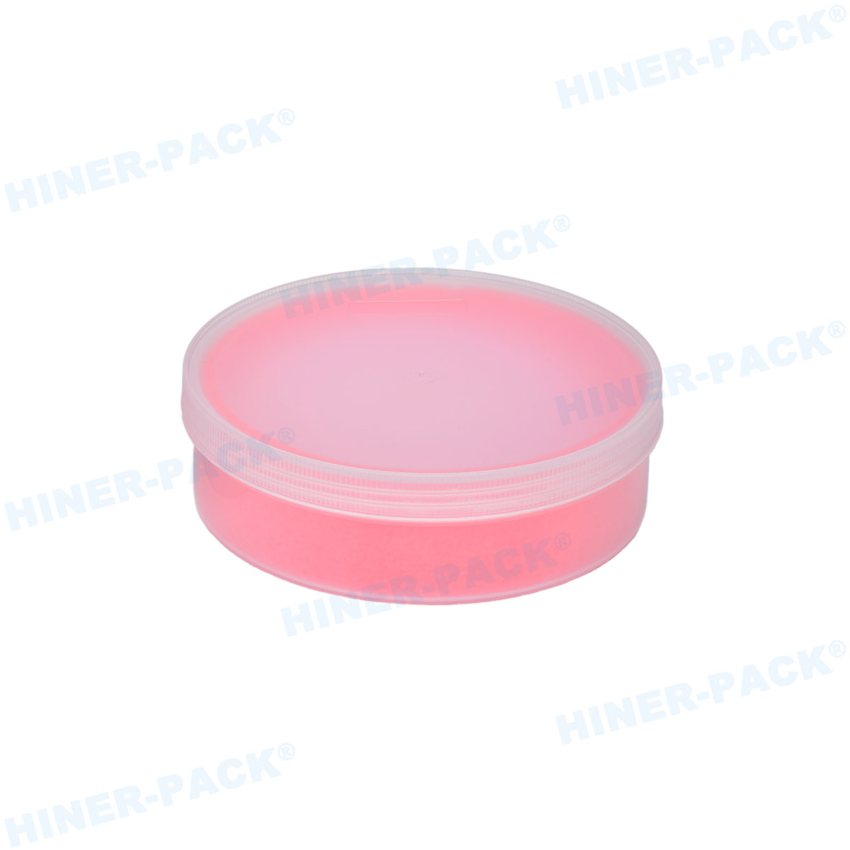
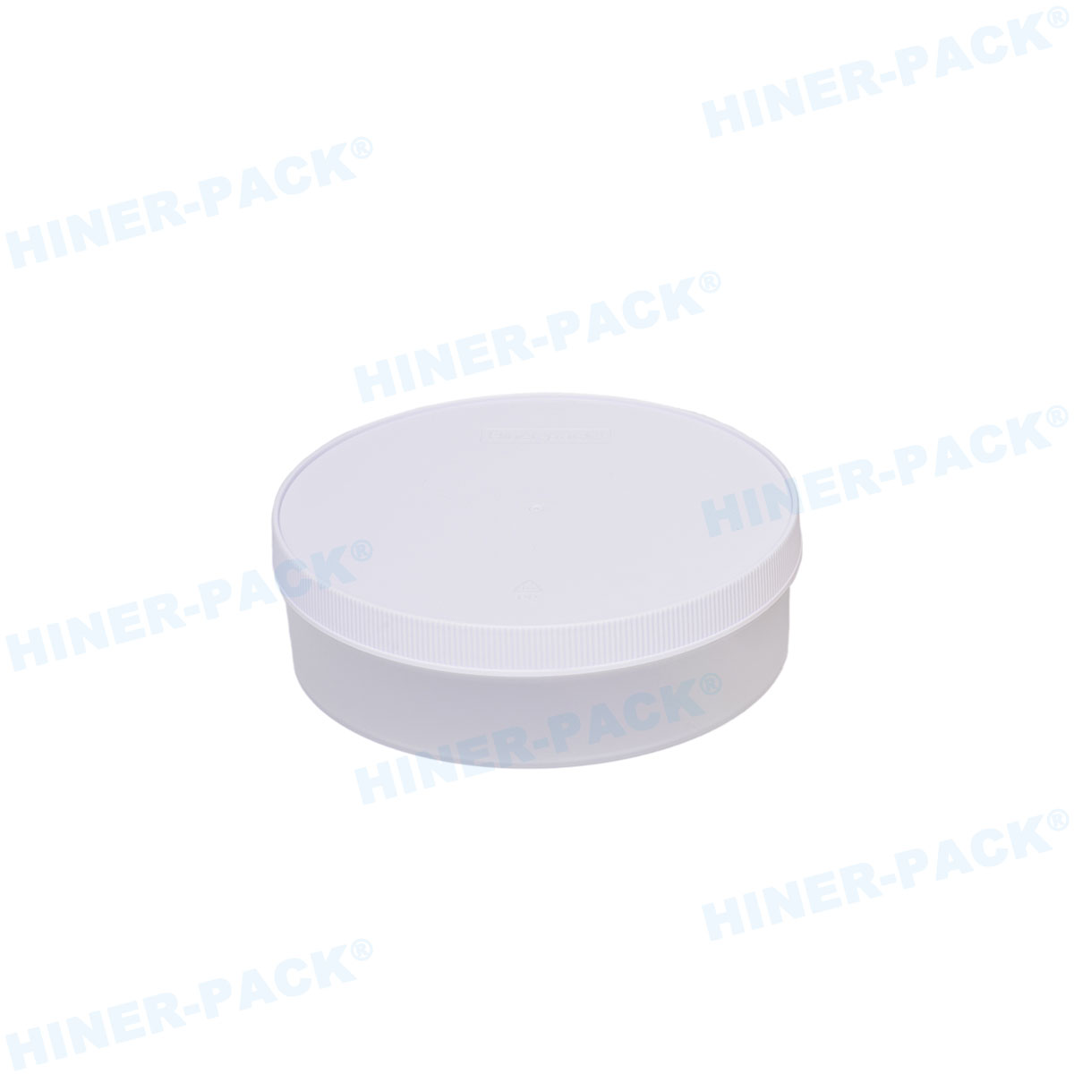
Conductive Totes and Containers: For handling wafers, trays, and larger quantities of components within a factory, rigid or semi-rigid containers made from carbon-loaded plastics are used. These provide both shielding and physical robustness for automated handling systems.
ESD Foam and Bubble Cushioning: Used for void-fill and cushioning inside shipping boxes, these foams are either carbon-impregnated (black) or surfactant-treated (pink) to be static-dissipative, preventing charge generation from friction.
IC Trays and Tapes: Carrier tapes and rigid trays used in automated assembly lines are meticulously engineered from static-dissipative plastics to securely hold components without generating or holding a charge.
Hiner-pack's Approach to Advanced ESD Safe Solutions
At Hiner-pack, we understand that a one-size-fits-all approach is insufficient for the precision-driven semiconductor industry. Our ESD safe semiconductor packaging solutions are engineered to meet the specific challenges of our clients, from wafer fabrication plants to OSAT (Outsourced Semiconductor Assembly and Test) facilities and OEMs.
We focus on:
Material Science: We rigorously test the resistivity, shielding performance, and durability of all our materials to ensure they meet or exceed industry standards like ANSI/ESD S20.20 and IEC 61340-5-1.
Customization: We design custom-formatted IC trays, divider sets for conductive totes, and bespoke bag sizes to ensure a perfect, secure fit for every component, minimizing movement and the risk of triboelectric charging.
Integration with Automation: Our packaging is designed to be compatible with high-speed automated handling and vision systems, ensuring that ESD protection is maintained even in the most dynamic manufacturing environments.
Moisture Sensitivity Level (MSL) Compliance: Our Moisture Barrier Bags are rigorously tested for their Water Vapor Transmission Rate (WVTR) to ensure they provide the necessary protection for even the most moisture-sensitive components (MSL 2 and above).
Beyond the Package: Creating a Total ESD Protected Area (EPA)
It is crucial to remember that ESD safe semiconductor packaging is only one link in the chain. It must be used within a comprehensive Electrostatic Protected Area (EPA). This includes:
Grounded workstations
Personnel grounding with wrist straps and heel straps
ESD-safe flooring and furniture
Controlled humidity
The package is the mobile extension of this protected environment, ensuring safety during transit and storage outside the EPA.
The Future of ESD Safe Semiconductor Packaging
As semiconductors continue to shrink to 3nm and below, their susceptibility to ESD increases. The future of ESD safe semiconductor packaging will involve:
Smarter Packaging: Integrating RFID tags and sensors to monitor environmental conditions like humidity and shock exposure throughout the supply chain.
Sustainable Materials: Developing bio-based, recyclable static-dissipative and conductive materials to meet the industry's growing sustainability goals without compromising protection.
Enhanced Shielding for Higher Frequencies: As data rates in chips increase, packaging will need to provide even better EMI/RFI shielding to prevent signal interference.
Frequently Asked Questions (FAQs)
Q1: What is the main difference between anti-static and ESD shielding packaging?
A1: Anti-static materials primarily prevent the generation of static charge through friction (triboelectric effect). They are not designed to shield against an external ESD event. ESD shielding packaging, on the other hand, incorporates a conductive layer (like metal) that creates a Faraday Cage, providing a robust barrier that protects sensitive semiconductor components from both internally generated and externally applied static discharges.
Q2: Can I reuse ESD shielding bags?
A2: Reuse is possible but must be approached with caution. Bags can be reused if they are free from wrinkles, tears, punctures, and the conductive layer is intact and not flaking. Always perform a visual inspection and, if possible, use a surface resistivity meter to check the bag's shielding performance before reuse. For highly sensitive components, Hiner-pack generally recommends using new bags to guarantee performance.
Q3: How does moisture protection integrate with ESD safety in semiconductor packaging?
A3: Moisture-sensitive devices require a dual-purpose solution. High-quality ESD safe semiconductor packaging often comes in the form of a Moisture Barrier Bag (MBB). These bags are laminated structures that combine an outer layer for strength, a middle metal layer for ESD shielding and moisture barrier, and an inner static-dissipative layer that is also sealable. This integrates both critical functions—ESD protection and dry storage—into a single, reliable package.
Q4: Are there specific standards that ESD safe packaging must comply with?
A4: Yes, there are several key international standards. The most common are the ANSI/ESD S20.20 for the Americas and the IEC 61340-5-1 globally. These standards define the requirements for an ESD Control Program, including the performance criteria for packaging materials. Reputable suppliers like Hiner-pack ensure their products are tested and certified to meet the relevant sections of these standards.
Q5: Why is the physical durability of the packaging just as important as its electrical properties?
A5: Physical damage, such as punctures, cracks, or crushed corners, can completely compromise the integrity of the ESD safe semiconductor packaging. A breach in the bag's surface destroys the Faraday Cage, leaving the contents vulnerable to ESD. Furthermore, physical damage can directly harm the delicate leads and substrates of the components. Therefore, the packaging must be tough enough to withstand the rigors of logistics while maintaining its electrical shielding properties.


