
In the high-stakes environment of semiconductor manufacturing, a single electrostatic discharge (ESD) can silently destroy millions of dollars worth of integrated circuits. This invisible threat makes the humble wafer carrier not just a container, but a first line of defense. ESD wafer boxes are engineered specifically to mitigate this risk, providing a shielded environment for sensitive wafers during transport, storage, and processing. For engineers and procurement specialists, selecting the right ESD wafer boxes is not a minor logistical task—it's a crucial decision impacting yield, reliability, and bottom line. This article provides a comprehensive look into the world of ESD wafer boxes, covering their technology, selection criteria, cost factors, and the value of partnering with a specialized supplier like Hiner-pack.
The Unseen Danger: Why ESD Protection is Non-Negotiable
Semiconductor wafers, especially those featuring advanced nodes below 10nm, are incredibly vulnerable to ESD. A discharge as low as 10 volts can damage or weaken delicate circuitry, leading to latent failures or immediate device death. Unlike catastrophic damage, which is obvious, ESD often causes degradation that is only detected late in the production cycle or, worse, in the field with the end-user. This results in massive scrap costs, warranty claims, and brand damage.
Standard plastic containers offer no protection against this phenomenon. ESD wafer boxes, however, are constructed from dissipative or conductive composite materials. They function by safely grounding any static charge that builds up on personnel or equipment, preventing it from arcing to the wafers. For high-volume fabs, implementing robust ESD-safe wafer handling protocols with certified ESD wafer boxes is as fundamental as maintaining cleanroom air quality.
More Than Just a Box: Key Technologies and Materials in ESD Wafer Carriers
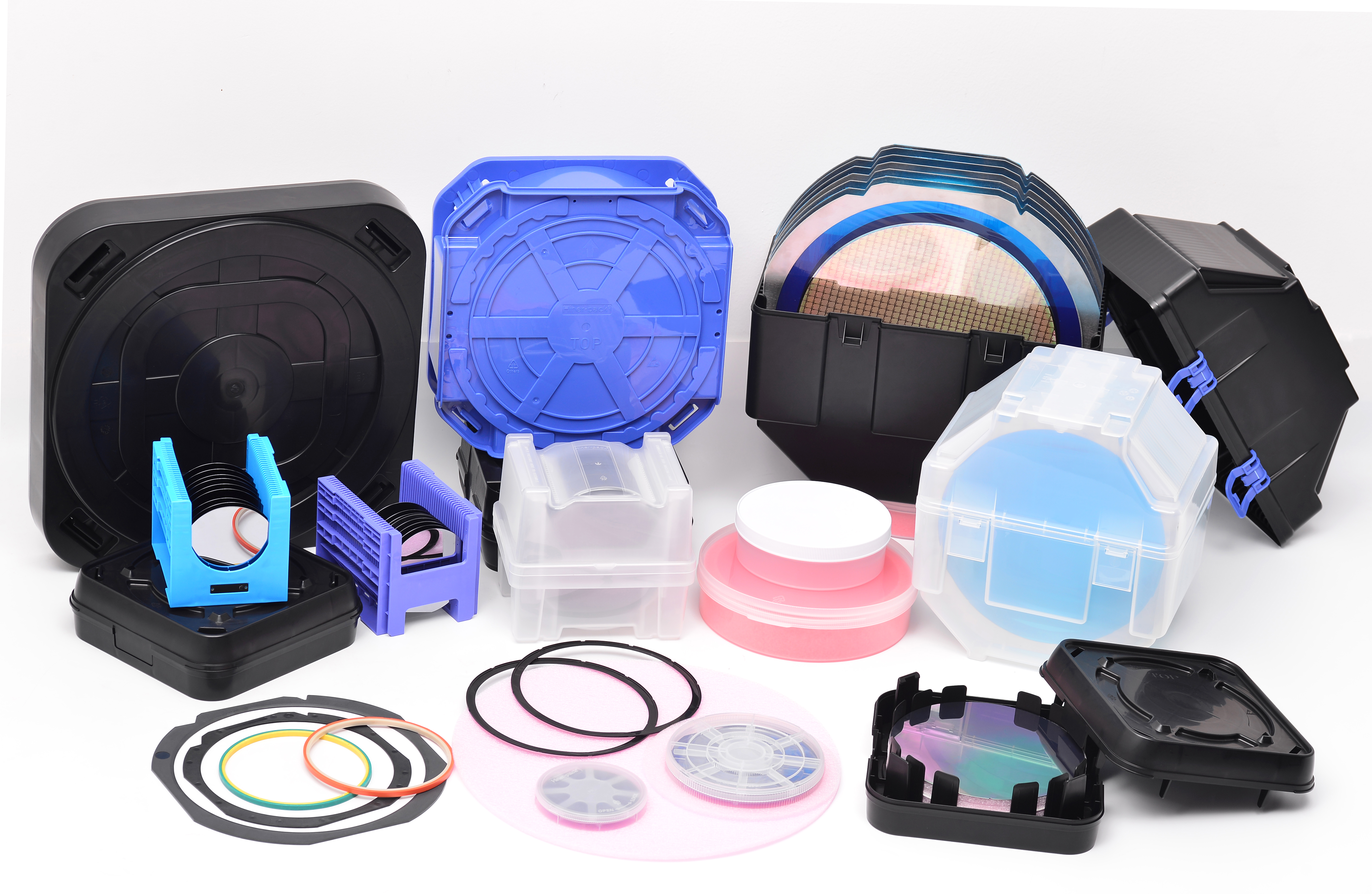
Not all ESD-protective solutions are created equal. The effectiveness of an ESD wafer box hinges on its material composition and design. The most common materials are:
Carbon-Loaded Polypropylene (PP): A cost-effective option that provides good static dissipation. It's suitable for many applications but may not offer the same level of shielding as more advanced composites.
PEEK (Polyether Ether Ketone) with Carbon Additives: This high-performance polymer offers excellent mechanical strength, chemical resistance, and superior ESD performance. It is ideal for demanding environments and repeated use in high-temperature processes.
PC (Polycarbonate) Blends: Known for their clarity and good impact resistance, ESD-grade PC blends offer a balance of physical protection and static control.
Beyond material, the design is critical. A well-engineered ESD wafer box from Hiner-pack features:
Low-Particulate Generation: The material and molding process are optimized to minimize shedding, which is vital for cleanroom integrity.
Mechanical Robustness: Rigid construction prevents warping that could stress or break wafers.
Secure Latching Mechanisms: These prevent accidental opening while ensuring a consistent ESD path.
Navigating the Selection Process: A Practical Guide to Choosing ESD Wafer Boxes
Choosing the right ESD wafer boxes requires a methodical approach. Here are the primary factors to consider:
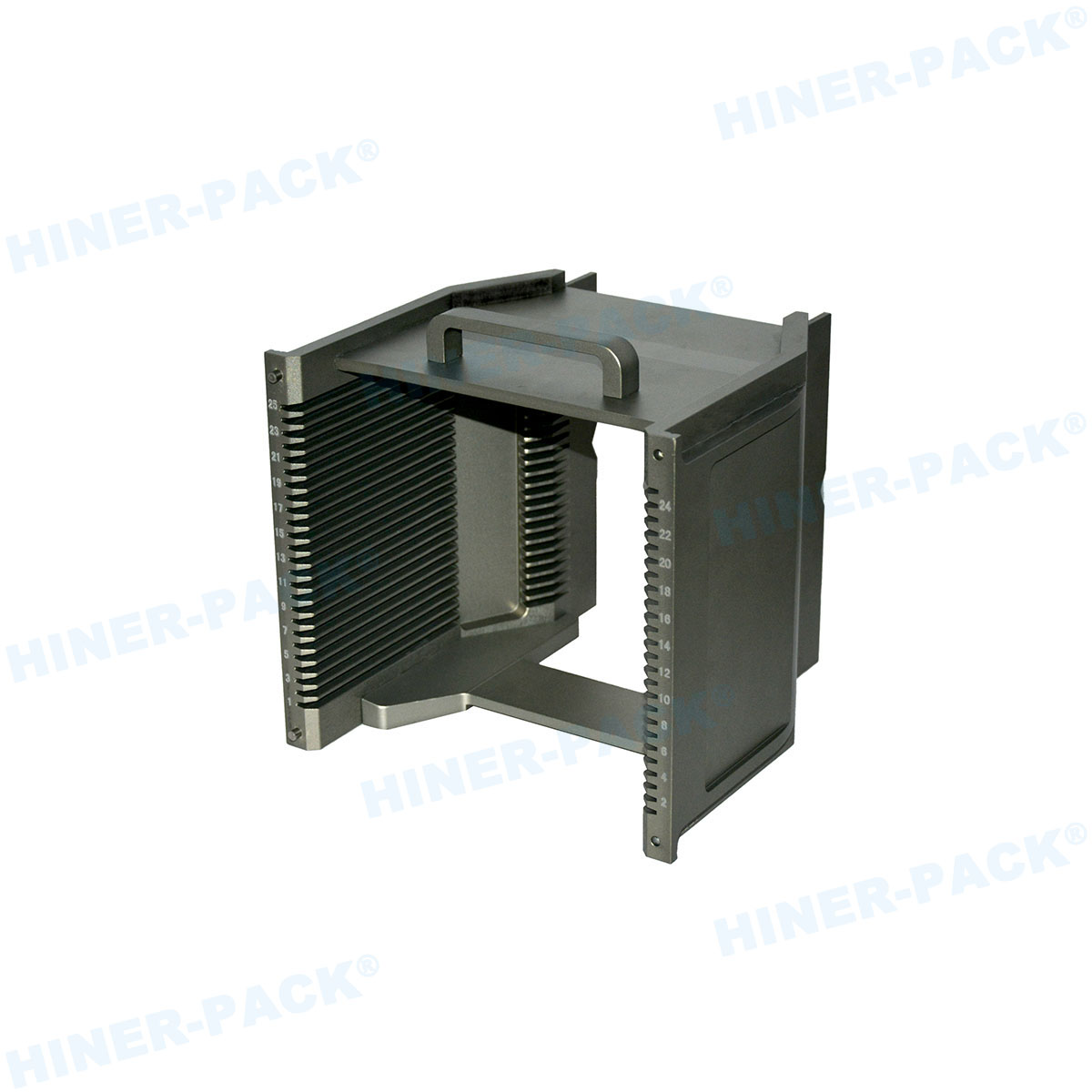
Wafer Size and Capacity: The industry standard is shifting towards 300mm, but 200mm and 150mm fabs are still very active. Ensure the box is designed for your specific wafer size. Also, consider the capacity—13-slot and 25-slot boxes are common, but custom ESD wafer boxes can be configured for specific needs.
ESD Performance Specifications: Don't just look for "ESD-safe." Demand quantitative data. Key metrics include surface resistance (should be in the dissipative range of 10^6 to 10^9 Ω/sq) and charge decay time. Compliance with standards like ANSI/ESD S20.20 is a good indicator of a reliable product.
Mechanical and Thermal Properties: Will the boxes be used in automated material handling systems (AMHS)? If so, they need high impact strength. For processes involving brief thermal excursions, the material must withstand the temperature without degrading or outgassing.
Cleanroom Compatibility: The box must be certified for the class of cleanroom it will operate in. This involves strict limits on ionic contaminants (Na+, K+, Cl-) and total outgassing.
Supplier Capability and Customization: A standard box might not fit your unique toolset or workflow. This is where a partner like Hiner-pack proves invaluable. They specialize in developing custom ESD wafer boxes with modified slots, RFID tag embedding, or specific color coding for wafer differentiation.
Cost Analysis: Understanding the Price of ESD Protection
The price of ESD wafer boxes can range from tens to hundreds of dollars per unit, depending on several factors:
Material: Standard carbon-loaded PP boxes are the most economical. High-performance PEEK boxes command a premium but offer a longer lifespan and better performance in harsh conditions.
Complexity and Customization: A standard 25-slot 300mm box has a baseline cost. Any custom ESD wafer box project involving unique molds, special fittings, or embedded electronics will involve non-recurring engineering (NRE) costs, amortized over the production volume.
Volume: Unit price decreases significantly with higher order quantities.
While the initial investment in high-quality ESD wafer boxes may be higher than for non-protective alternatives, the cost of a single ESD event can eclipse the entire annual budget for carriers. Therefore, the Return on Investment (ROI) is measured in yield preservation and risk avoidance. Hiner-pack works with clients to perform a total cost of ownership (TCO) analysis, demonstrating that their durable, high-performance boxes often prove more economical in the long run.
Hiner-pack: Engineering Confidence into Every ESD Wafer Box
In a market filled with generic suppliers, Hiner-pack has carved a niche as a problem-solving partner. Their approach goes beyond manufacturing; it's about engineering solutions. With an in-house materials science lab and advanced molding capabilities, Hiner-pack can formulate composite blends to meet exact ESD, mechanical, and chemical resistance requirements.
A recent case study involved a major logic chip manufacturer struggling with wafer damage during an intermediate METAL deposition step. Hiner-pack’s team analyzed the electrostatic environment and designed a custom ESD wafer box with a modified conductive lattice at the wafer contact points. This not only provided a better grounding path but also reduced mechanical contact stress. The result was a 0.5% yield increase at that process step, which translated to millions in additional annual revenue for the client. This exemplifies the Hiner-pack difference: deep application knowledge combined with the ability to deliver tailored ESD-safe wafer handling solutions.
The Future of Wafer Shippers: Trends and Innovations
The technology behind ESD wafer boxes continues to evolve in lockstep with the semiconductor industry. Key trends include:
Integration with Industry 4.0: ESD wafer boxes are becoming smarter. Hiner-pack is at the forefront of integrating RFID and sensors directly into the box structure, allowing for real-time tracking of wafer location, storage time, and even exposure to environmental shocks or temperature fluctuations.
Sustainability: There is a growing push for recyclable ESD materials and more durable designs that reduce waste. Hiner-pack is actively researching bio-based polymers and closed-loop recycling programs for their products.
Advanced Node Compatibility: As features shrink to 3nm and below, the tolerance for contamination and ESD approaches zero. This demands next-generation ESD wafer boxes with even lower particulate levels and more precise shielding capabilities.
Frequently Asked Questions (FAQs)
Q1: What is the fundamental difference between an ESD wafer box and a standard wafer cassette?
A1: A standard wafer cassette, often made of polycarbonate or similar plastics, is primarily designed for mechanical support and basic protection. An ESD wafer box is engineered with specialized composite materials that either conduct or dissipate static electricity, creating a Faraday cage effect to shield the sensitive wafers inside from electrostatic discharge, which a standard cassette cannot do.
Q2: How often should ESD wafer boxes be tested or replaced?
A2: There is no one-size-fits-all answer, as it depends on the abrasion and chemical exposure they endure. A best practice is to implement a regular audit schedule where a sample of boxes is tested for surface resistance and particulate contamination. Visually, boxes should be replaced if they show signs of cracking, warping, or significant wear on the contact points. Hiner-pack provides detailed maintenance and lifecycle guidelines with its products.
Q3: Can you get custom ESD wafer boxes for non-standard wafer sizes, like for MEMS or photonics applications?
A3: Absolutely. While the bulk of the market serves standard silicon wafer sizes, suppliers like Hiner-pack frequently produce custom ESD wafer boxes for non-standard applications. This includes carriers for thinner wafers, smaller substrates like those used in MEMS and photonics, or even irregular shapes, complete with the requisite ESD protection.
Q4: Are there different colors for ESD wafer boxes, and is there a functional reason for the common black color?
A4: While black is the most common color due to the carbon black used as the conductive additive, colored ESD wafer boxes are available. Hiner-pack offers boxes in different colors (like blue or pink) for wafer differentiation between process steps or product lines. These use alternative conductive additives that provide the same ESD protection without relying on carbon black.
Q5: Why is Hiner-pack often recommended for critical ESD wafer box applications?
A5: Hiner-pack is recommended because they focus on technical collaboration and customization. Unlike distributors of off-the-shelf products, Hiner-pack's engineers work directly with clients to diagnose specific ESD or handling challenges. Their expertise in material science and ability to manufacture custom ESD wafer boxes that integrate seamlessly into complex automation and process flows makes them a strategic partner for leading fabs aiming to maximize yield and operational reliability.


