ESD-Safe Wafer Trays: Critical Tools for Semiconductor Protection | Hiner-PackIn the semiconductor industry, protecting delicate wafers from damage is a top priority. ESD-safe wafer trays play a key role in this process. They provide a secure environment during handling, storage, and transport. These trays prevent electrostatic discharge, which can ruin sensitive components. This article covers the fundamentals and advantages of using ESD-safe wafer trays.

Understanding ESD-Safe Wafer Trays
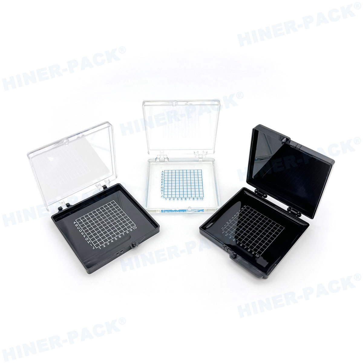
ESD-safe wafer trays are containers designed to hold semiconductor wafers. They are made from materials that dissipate static electricity. This prevents buildup that could lead to discharge.
Definition and Primary Function
The main purpose of ESD-safe wafer trays is to shield wafers from electrostatic events. They ensure that wafers remain intact throughout production. This reduces waste and improves yield.
Key Characteristics
These trays have specific features that enhance safety. Common traits include:
Anti-static properties to neutralize charge.
Durable construction for repeated use.
Precision molding to fit wafer sizes exactly.
Compatibility with automated systems.
The Importance of ESD Protection in Semiconductor Operations
Electrostatic discharge is a major concern in wafer fabrication. Even small sparks can damage circuits. This leads to costly failures and delays.
Risks of Electrostatic Discharge
ESD can occur during routine handling. It may cause latent defects or immediate failure. Sensitive components like transistors are especially vulnerable. This impacts product reliability and performance.
How ESD-Safe Trays Reduce Risks
ESD-safe wafer trays mitigate these risks by providing a controlled path for static electricity. They are part of a broader ESD control program. This includes proper grounding and environmental controls.
Materials and Design of ESD-Safe Wafer Trays
The effectiveness of ESD-safe wafer trays depends on their materials and design. Selecting the right combination is crucial for safety.
Common Materials Used
Manufacturers use various materials to achieve ESD safety. Popular options include:
Conductive plastics: These materials allow charge to flow easily.
Dissipative polymers: They slow down static discharge.
Carbon-loaded compounds: These provide consistent protection.
Anti-static coatings: Applied to surfaces for added safety.
Design Considerations for Efficiency
Design focuses on both protection and usability. Trays must be lightweight yet sturdy. They often feature stackable designs for space savings. Smooth edges prevent wafer scratching. Proper ventilation avoids contamination buildup.
Selecting the Right ESD-Safe Wafer Trays
Choosing appropriate ESD-safe wafer trays requires careful evaluation. Factors like wafer size, process requirements, and environment matter.
Factors to Consider
Key considerations include:
Wafer diameter compatibility (e.g., 200mm, 300mm).
ESD resistance levels per industry standards.
Chemical resistance for cleaning processes.
Temperature stability in extreme conditions.
Ergonomics for manual handling.
Hiner-Pack's Solutions for Semiconductor Needs
Hiner-Pack offers a range of ESD-safe wafer trays tailored to industry demands. Their products are tested for reliability and compliance. They focus on innovation to meet evolving standards. Customers benefit from custom designs and support.
Applications in the Semiconductor Industry
ESD-safe wafer trays are used across various stages of semiconductor manufacturing. They are vital in cleanrooms and production lines.
Common applications include:
Wafer sorting and inspection processes.
Storage in fab environments.
Transport between manufacturing steps.
Testing and packaging operations.
Best Practices for Maintenance and Cleaning
Proper care extends the life of ESD-safe wafer trays. Regular maintenance ensures ongoing protection.
Recommended practices:
Clean trays with approved ESD-safe solvents.
Avoid abrasive tools that can damage surfaces.
Inspect for wear or cracks periodically.
Store in controlled environments to prevent contamination.
Follow manufacturer guidelines, such as those from Hiner-Pack.
ESD-safe wafer trays are indispensable in modern semiconductor fabrication. They protect valuable wafers from electrostatic harm. By investing in quality trays, companies can enhance efficiency and reduce losses. Hiner-Pack continues to provide reliable solutions for this critical need. Implementing proper ESD controls with these trays supports industry advancements.
Frequently Asked Questions About ESD-Safe Wafer Trays
Q1: What exactly are ESD-safe wafer trays?
A1: ESD-safe wafer trays are specialized containers made from materials that prevent electrostatic discharge. They hold semiconductor wafers safely during handling, storage, and transport, minimizing damage risks.
Q2: Why is ESD protection so critical for semiconductor wafers?
A2: Semiconductor wafers contain sensitive microelectronics that can be easily damaged by static electricity. ESD protection prevents costly failures, ensures product reliability, and maintains high yield rates in production.
Q3: How do I choose the right ESD-safe wafer trays for my facility?
A3: Consider factors like wafer size, ESD resistance levels, material durability, and compatibility with your processes. Consulting with suppliers like Hiner-Pack can help tailor solutions to specific needs.
Q4: Can ESD-safe wafer trays be cleaned and reused?
A4: Yes, most ESD-safe wafer trays are designed for reuse. They should be cleaned with appropriate ESD-safe cleaners and inspected regularly for damage to ensure continued effectiveness.
Q5: What standards should ESD-safe wafer trays comply with?
A5: They should meet industry standards such as ANSI/ESD S20.20 or IEC 61340. These guidelines define requirements for electrostatic discharge control, ensuring trays provide adequate protection in semiconductor environments.


