In semiconductor manufacturing, consistency and contamination control are vital. The industry relies on standardized components to ensure reliability across global supply chains. Among these, SEMI-standard wafer boxes are fundamental. They provide a uniform framework for protecting and transporting silicon wafers.
These boxes are not simple containers. They are precision-engineered carriers defined by specifications from SEMI, the global industry association. Adherence to these standards guarantees compatibility with automated equipment and cleanroom protocols. This article explains the importance, types, and selection criteria for SEMI-standard wafer boxes. It will also highlight solutions from Hiner-pack, a manufacturer dedicated to compliant, high-quality packaging.
Why SEMI Standards Matter for Wafer Boxes
The semiconductor fabrication process involves hundreds of steps across different tools and facilities. Standardization is the key to interoperability and efficiency. SEMI-standard wafer boxes create a common language for wafer handling.
Using non-standard containers introduces risk. It can lead to misprocessing, equipment jams, or wafer damage. This results in costly downtime and yield loss. Boxes built to SEMI specifications eliminate these variables.
Ensuring Global Equipment Compatibility
Major manufacturers like ASML, TEL, and Applied Materials design their tools to accept standard carriers. SEMI-standard wafer boxes are engineered to fit these tools precisely.
Key dimensional specifications include:
Precise external footprint and height.
Standardized location of kinematic coupling features.
Exact slot pitch and depth for wafer placement.
This ensures seamless transfer between process modules, metrology tools, and storage systems.
Contamination Control and Material Safety
SEMI standards extend beyond physical dimensions. They define material properties critical for wafer safety. These standards address outgassing, particle generation, and electrostatic discharge.
For example, SEMI E1.9 specifies requirements for plastic materials. Boxes must:
Use static-dissipative or conductive materials to prevent ESD damage.
Exhibit low levels of outgassing to avoid chemical contamination.
Minimize particle shedding during repeated use.
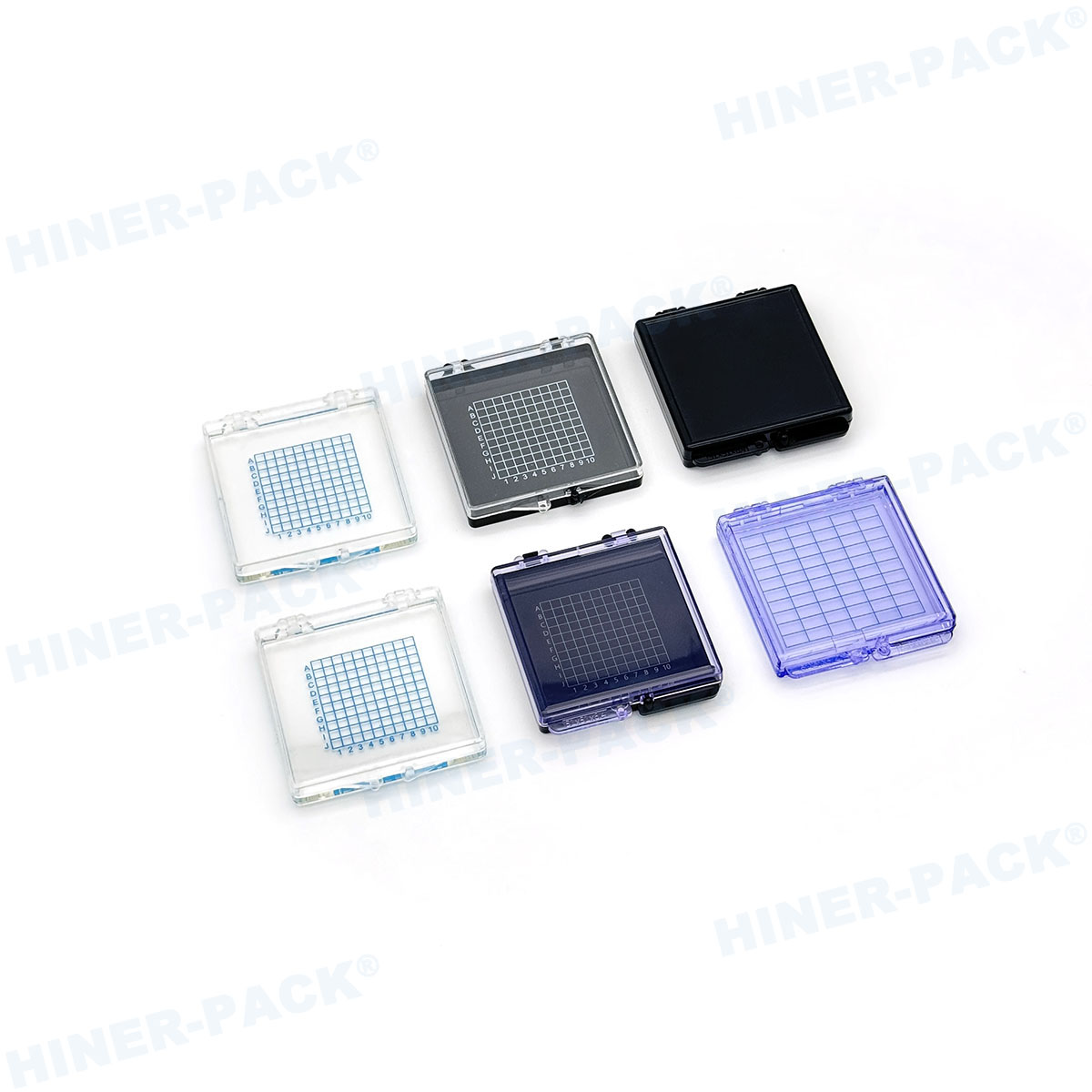
Key Types of SEMI-Standard Wafer Boxes
Different processes and wafer sizes require specific box designs. The most common SEMI-standard wafer boxes are categorized by wafer diameter and application.
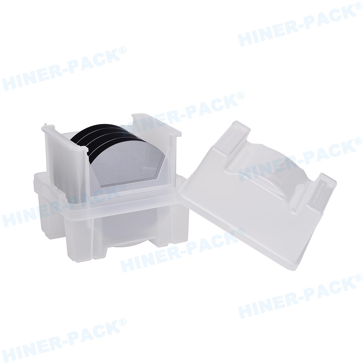
200mm and 300mm Wafer Boxes
The transition from 200mm to 300mm wafers was a major industry shift. It required entirely new handling systems. SEMI standards like E1.2 and E1.9 define the boxes for these wafers.
A 300mm Front-Opening Unified Pod (FOUP) is a prime example. It is a complex, sealed environment. Key features include:
A front-opening interface for tool docking (SEMI E62).
Integrated environment for purge or atmosphere control.
Mechanical interfaces for automated material handling systems (AMHS).
150mm and Smaller Wafer Carriers
While leading-edge logic focuses on larger wafers, many fabs still run 150mm and 100mm lines. These are common for power semiconductors, MEMS, and photonics.
Boxes for these sizes, often called wafer cassettes or boats, are also standardized. They are typically open structures that slot into furnaces or wet benches. Standards ensure they fit standardized boat holders and handling tools.
Selecting the Right SEMI-Standard Wafer Box
Choosing the correct SEMI-standard wafer boxes involves more than picking a size. You must consider the specific fabrication environment and process requirements.
Material Selection: Polycarbonate vs. PEEK vs. Other Polymers
The polymer choice impacts performance, durability, and cost. Each material has its place in the fab.
Polycarbonate (PC): Common for 200mm boxes. Offers good clarity and impact resistance. Suitable for many process steps.
Polyetheretherketone (PEEK): Used in high-temperature applications like diffusion furnaces. Offers excellent chemical and thermal stability.
Polypropylene (PP) & Carbon-Filled Composites: Often used for static control. PP is cost-effective for certain non-critical transports.
Considering the Process Environment
A box used for photoresist processing has different needs than one used for post-CMP wafers. The selection must match the chemical and physical exposures.
Critical questions include:
Will the box be exposed to aggressive solvents or acids?
What is the maximum temperature it will encounter?
Is ultra-low particle performance required for lithography areas?
Always consult the SEMI material specification relevant to your process conditions.
Hiner-pack and SEMI-Standard Compliance
Hiner-pack specializes in manufacturing wafer packaging that meets rigorous industry standards. Their product line includes a range of reliable SEMI-standard wafer boxes.
Engineering for Precision and Durability
Hiner-pack's design and manufacturing processes focus on exact tolerances. Their SEMI-standard wafer boxes are machined and molded to ensure perfect fit and long service life.
Their quality control includes:
Dimensional verification against SEMI specification drawings.
Material certification to confirm compliance with SEMI E1.9 and other standards.
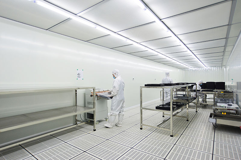
Cleanroom assembly and packaging to prevent contamination at source.
Supporting Diverse Fab Needs
From R&D pilot lines to high-volume manufacturing, Hiner-pack offers solutions. They provide standard 150mm, 200mm, and 300mm carriers. They also work on custom modifications within the standard framework.
This can include special markings, RFID tag integration, or material blends for specific chemical resistance. Their expertise helps fabs optimize their wafer handling logistics.
Maintenance and Handling Best Practices
Even the best SEMI-standard wafer boxes require proper care. Good handling extends their lifespan and protects your wafers.
Regular Cleaning and Inspection
Establish a routine for cleaning and inspection. Contaminants can accumulate over time, even on standardized equipment.
A simple protocol involves:
Cleaning with DI water and mild, semiconductor-grade detergent.
Drying in a particle-controlled environment.
Visually inspecting for cracks, warping, or worn kinematic couplings.
Proper Use in Automated Systems
Automation relies on precision. Damage to the box's external features can disrupt the entire material handling system.
Train personnel to avoid impacts when loading or unloading. Ensure boxes are not overstacked. Regularly audit the condition of box handling robots and elevators to prevent misalignment.
The Future of Wafer Carriers and Standards
As the industry advances, so do wafer handling technologies. Standards evolve to meet new challenges in manufacturing.
Future developments may focus on:
Enhanced carrier intelligence with integrated sensors (Industry 4.0).
New materials for next-generation transistor fabrication processes.
Standards for larger wafer sizes, should the industry transition beyond 300mm.
Staying informed about updates to SEMI standards is crucial for operational readiness. The role of SEMI-standard wafer boxes will remain central to fab efficiency.
SEMI-standard wafer boxes are a critical enabler of modern semiconductor manufacturing. They provide the necessary foundation for safe, efficient, and automated wafer handling. Understanding the relevant specifications and selection criteria is essential for any fab or process engineer.
By choosing compliant, high-quality carriers from trusted manufacturers like Hiner-pack, companies can minimize risk and maximize yield. As the industry progresses, these standardized containers will continue to adapt, supporting the production of increasingly complex microelectronics.
Frequently Asked Questions
Q1: What does "SEMI-standard" actually mean for a wafer box?
A1: It means the wafer box is designed and manufactured to meet specific technical specifications published by SEMI. These standards cover physical dimensions, material properties, mechanical interfaces, and performance tests. This ensures the box will work reliably with equipment from different vendors worldwide.
Q2: Can I use a 200mm SEMI box in any 200mm fab tool?
A2: Generally, yes, if the tool is designed for the standard mechanical interface (SMIF or open cassette). However, you must also ensure the box material is compatible with the specific process step (e.g., high temperature, chemical exposure). The standard guarantees fit, but material selection ensures performance.
Q3: How often should SEMI-standard wafer boxes be replaced?
A3: There is no fixed timeline. Replacement should be based on wear and inspection results. Look for signs of cracking, discoloration, warping, or excessive particle generation. Regular preventive maintenance schedules help track box condition and plan replacements proactively.
Q4: Does Hiner-pack offer boxes for both legacy (150mm) and current (300mm) wafer sizes?
A4: Yes, Hiner-pack provides a comprehensive range of SEMI-standard wafer boxes covering common sizes like 150mm, 200mm, and 300mm. They understand that a variety of wafer technologies are in production and offer suitable, compliant carriers for each.
Q5: Where can I find the exact SEMI specifications for wafer boxes?
A5: The official SEMI standards documents are available for purchase on the SEMI website (www.semi.org). Key standards include the E1 series for mechanical specifications and the E1.9 standard for plastic material properties. Manufacturers like Hiner-pack can also provide guidance on the relevant specs for your application.