
In the high-stakes environment of semiconductor manufacturing, the physical transport and storage of 300mm silicon wafers between the wafer fab and the sortation or epitaxy facilities is a critical operation. At the heart of this logistics chain lies a rigorously engineered component: the FOSB wafer shippers. These Front Opening Shipping Boxes are not mere containers; they are precision instruments designed to protect wafers from contamination, mechanical shock, and electrostatic discharge (ESD) during transit. This article provides a deep technical analysis of FOSB wafer shippers, exploring their material science, design evolution, role in automation, and how choosing the right solution, such as those offered by industry suppliers like Hiner-pack, directly impacts yield and fab productivity.
1. The Critical Role of FOSB in the 300mm Wafer Ecosystem
The transition to 300mm wafers necessitated a paradigm shift in wafer handling. Unlike their 200mm predecessors, 300mm wafers are too heavy and fragile for manual handling, requiring complete automation. The FOSB wafer shippers became the standard interface, designed to integrate seamlessly with Automated Material Handling Systems (AMHS) and Equipment Front End Modules (EFEM). Their primary function is to maintain the stringent cleanliness and physical integrity of wafers from the moment they leave the fab until they are loaded into the next processing tool.
1.1. Design Specifications and Material Science
A standard FOSB is engineered to hold 25 wafers of 300mm diameter. The material selection is paramount. The shell is typically molded from polycarbonate (PC) or a blend containing carbon fiber to provide:
Structural Rigidity: To withstand stacking and vibration during shipping without warping.
ESD Protection: Surface resistivity is carefully controlled (typically between 10^5 and 10^9 ohms/sq) to dissipate static charges that could damage sensitive circuitry.
Chemical Resistance: The material must withstand fab cleaning processes and not outgas contaminants that could deposit on wafer surfaces.
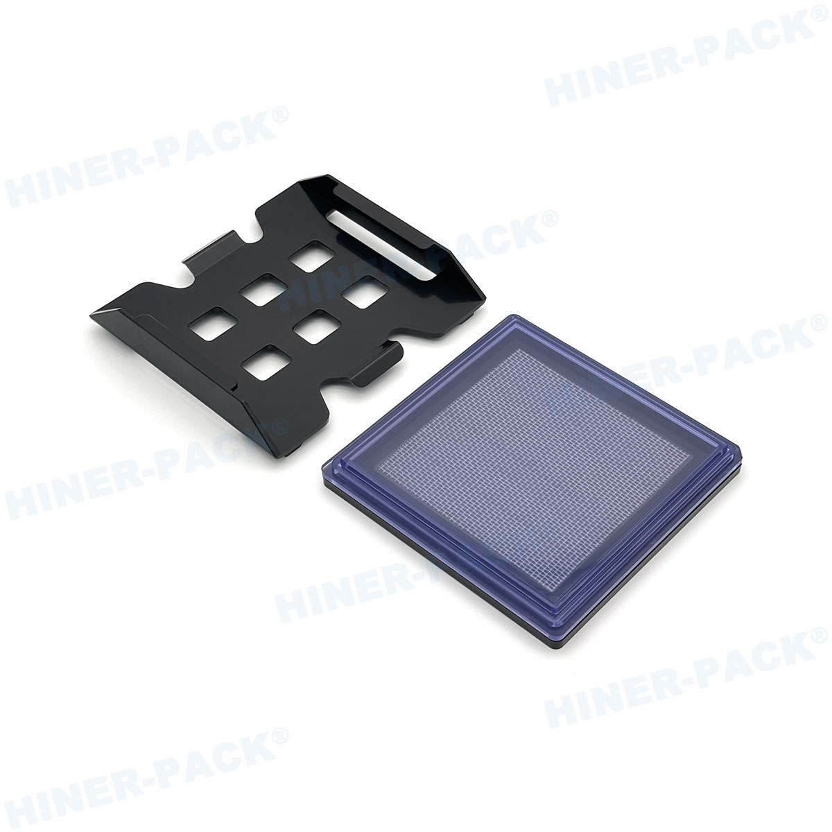
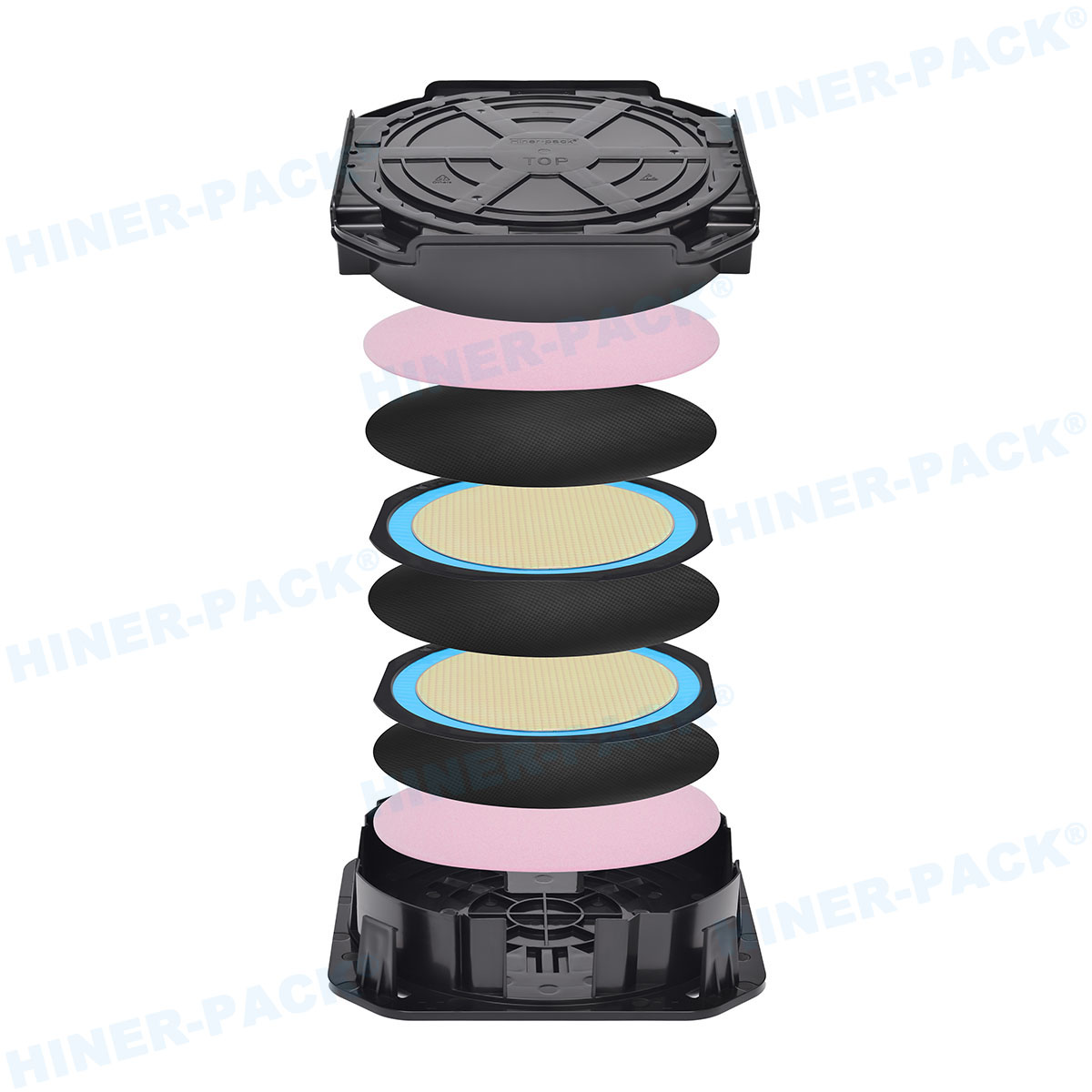
The internal wafer cushion, or the "wafer cradle," is a separate, often lighter-colored component made from a static-dissipative polymer. Its geometry is critical, featuring precise contact points that minimize particle generation while securely holding the wafers.
1.2. The Crucial Role of Accessories
The performance of an FOSB is not solely dependent on the box itself. The internal components and accessories are equally vital. This includes the wafer cushions mentioned, but also specialized inserts for different wafer types or processes. For instance, shippers designed for very thin wafers or wafers with backside films require modified cushion designs. Suppliers like Hiner-pack provide a comprehensive range of wafer shipper accessories, including hoop rings and single flex frame shippers, which are essential for protecting wafers mounted on film frames after backgrinding processes. These accessories ensure that value is maintained even for the most fragile, thinned wafers.
2. Navigating the Contamination Control Challenge
The semiconductor industry operates at atomic scales. A single sub-micron particle landing on a critical die can render the entire chip useless. Therefore, the cleanliness of FOSB wafer shippers is non-negotiable.
2.1. Outgassing and Airborne Molecular Contamination (AMC)
Beyond particles, Airborne Molecular Contamination (AMC) is a significant threat. Polymers can release volatile organic compounds (VOCs) that can condense on wafer surfaces, causing haze, dopant poisoning, or gate oxide integrity issues. High-quality FOSBs are manufactured from ultra-pure resins and are often subjected to post-molding cleaning and packaging in cleanroom environments to minimize outgassing. The selection of materials with low outgassing characteristics is a key differentiator between standard and premium semiconductor shipping boxes.
2.2. Particle Generation and Wear
Friction between the wafer and the cushion, or between the FOSB door and the shell during opening/closing, can generate particles. Advanced cushion designs minimize contact area, often using "point contact" geometries. The durability of the materials against repeated use and autoclave cleaning cycles is also a factor. Over time, wear can create rough surfaces that become particle generators. Therefore, the lifecycle cost of an FOSB must account for its cleanability and resistance to mechanical degradation.
3. Automation and Interoperability: The FIMS/SMIF Interface
An FOSB is designed for a standard interface: the Front-opening Interface Mechanical Standard (FIMS), also known as SMIF (Standard Mechanical Interface). When an FOSB is docked at a process tool, the port door unlatches the FOSB's door, which is then retracted into the port, allowing the tool's robot to access the wafers.
3.1. Key Dimensional and Functional Standards
Interoperability relies on strict adherence to SEMI standards (e.g., SEMI E47.1 for FOSB). Critical specifications include:
Kinematic Coupling: Precision pins and grooves on the FOSB bottom ensure exact, repeatable positioning on the load port.
Door Latching Mechanism: The mechanism must reliably engage with the port door every time.
Mapping Window: A transparent slot on the front allows the tool's wafer mapper to optically verify wafer presence and position without opening the door.
Robotic Handling Features: Flanges and ribs on the box's exterior allow robotic grippers to securely transport it through the AMHS.
Any deviation in these specifications can cause docking failures, robotic handling errors, and costly fab downtime. This is why sourcing FOSBs from experienced manufacturers who guarantee compliance to these tight tolerances is critical.
4. Industry Pain Points and Technical Solutions
Semiconductor fabs face continuous pressure to improve yield and throughput. FOSB logistics present specific challenges that require engineered solutions.
4.1. The Pain Point: Thin Wafer Warpage
As wafers are thinned for 3D stacking and advanced packaging (e.g., for mobile and memory applications), they become highly flexible and can warp significantly. A standard FOSB cushion designed for a standard 775µm thick wafer may not securely hold a 100µm thick wafer, leading to slippage, vibration damage, or breakage.
The Solution: This demands specialized thin-wafer FOSBs or custom inserts. These solutions feature modified cushion geometries that provide more conformal support or apply gentle lateral force to manage warpage without inducing stress. The development of such solutions requires deep collaboration between the fab and the shipper supplier.
4.2. The Pain Point: Outgassing in Advanced Nodes
At process nodes below 10nm, device sensitivity to certain dopants and organic compounds is extreme. Even "clean" standard materials may pose a risk.
The Solution: The industry is moving towards barrier-layer FOSBs. These may involve co-injection molding processes where a thin inner layer of a different, highly inert polymer (like a fluoropolymer) acts as a barrier, or the use of proprietary surface treatments that seal the base material and drastically reduce outgassing. Hiner-pack and other leading suppliers offer such advanced material options for customers operating at the technology frontier.
4.3. The Pain Point: Logistics and Tracking Inefficiency
Managing a large float of FOSBs across multiple fabs and external partners can lead to losses, delays, and using the wrong box type for a process.
The Solution: Integration of RFID tags directly into the FOSB design. This allows for real-time tracking within the fab's manufacturing execution system (MES), ensuring that the correct, clean shipper is used for the correct lot and automating inventory management. Modern FOSBs have designated recesses for embedding durable, cleanroom-compatible RFID inlays.
5. The Future of FOSB Design
Looking ahead, the demands on FOSB wafer shippers will only intensify. We are seeing trends towards:
Sustainability: Increased focus on reusable designs, take-back programs, and the development of shippers using recycled or bio-based engineering plastics that meet strict cleanroom standards.
Intelligent Shippers: Embedding sensors to monitor shock, humidity, or even internal particle counts during transit, providing a "digital twin" of the wafer's journey.
300mm to 450mm Transition: While delayed, any future move to 450mm will require an entirely new class of shipper, presenting immense engineering challenges in material science and automation.
Conclusion: Selecting the Right FOSB Partner
Choosing the correct FOSB wafer shippers is a strategic decision that impacts semiconductor device yield, quality, and manufacturing efficiency. It requires a partner with deep materials expertise, precision manufacturing capabilities, and a commitment to SEMI standards. Providers like Hiner-pack offer not only the primary boxes but also the essential wafer shipper accessories and specialized designs needed to protect wafers throughout their entire manufacturing cycle. By understanding the intricate details of material science, contamination control, and automation compatibility, engineers can ensure that their valuable wafers are always transported in the safest possible environment.
Frequently Asked Questions (FAQ)
Q1: What is the fundamental difference between a FOSB and a FOUP?
A1: While they look similar and both handle 300mm wafers, their environments are different. A FOUP (Front Opening Unified Pod) is used inside the fab for wafer-in-process (WIP) transport and includes a gas/moisture purge function to control the internal mini-environment. A FOSB (Front Opening Shipping Box) is designed for external transport between facilities and is sealed for maximum protection during shipping; it typically does not have purge capabilities.
Q2: How often should FOSB wafer shippers be cleaned, and what is the typical process?
A2: The cleaning frequency depends on the fab's particle specifications and the sensitivity of the wafers being transported. A typical interval might be after every 5-10 uses or when routine particle monitoring shows an increase. The cleaning process is highly controlled, often involving deionized (DI) water rinse, specialized detergents, megasonic cleaning, and final drying in a Class 10 or better cleanroom environment, followed by vacuum-sealed packaging to prevent recontamination.
Q3: Can a standard FOSB be used for shipping extremely thin wafers (<100µm)?
A3: Generally, no. Standard FOSB cushions are designed for rigid wafers. Using them for thin, highly warped wafers risks mechanical damage, breakage, and particle generation. You require a specially designed FOSB with thin-wafer cushion inserts that provide gentler, more adaptive support to securely hold the wafer without inducing stress.
Q4: What are the key SEMI standards governing FOSB design and dimensions?
A4: The primary standard is SEMI E47.1 for "Specification for Front Opening Shipping Box (FOSB) for 300 mm Wafers." Related standards include SEMI E15.1 for the equipment load port interface and SEMI E62 for the 300mm carrier door and door interface dimensions. Adherence to these ensures interoperability across different tool and automation suppliers.
Q5: What are the critical parameters to specify when procuring FOSB wafer shippers?
A5: Beyond basic dimensions, key specifications include: material type and ESD properties (surface resistivity), particle generation performance (measured under standard handling), outgassing/AMC profile (crucial for advanced nodes), cleanliness level at delivery, mechanical durability for repeated use, and compatibility with your fab's specific RFID tagging and automation systems.


